
Overlay measurement method and system in integrated circuit chip manufacturing process

A technology of overlay measurement and manufacturing process, applied in the field of overlay measurement, which can solve problems such as lens distortion, overlay error, wafer stage shaking, etc., to improve stability and accuracy, improve measurement efficiency, and shorten measurement time Effect

Active Publication Date: 2021-07-23
普赛微科技(杭州)有限公司
View PDF5 Cites 0 Cited by
  • Summary
  • Abstract
  • Description
  • Claims
  • Application Information

AI Technical Summary

Problems solved by technology

In addition to the above-mentioned overlay errors, other factors, such as graphic magnification, lens distortion, wafer stage shaking, etc., may also cause overlay errors between different process levels
[0005] Various defects that may occur during chip manufacturing, these defects may affect the stability and accuracy of the overlay measurement process
In addition, due to the limitation of equipment production capacity and measurement time, usually only the overlay marks in some areas on the wafer can be measured, and the overlay data in other areas cannot be directly obtained

Method used


Image

  • Overlay measurement method and system in integrated circuit chip manufacturing process
  • Overlay measurement method and system in integrated circuit chip manufacturing process
  • Overlay measurement method and system in integrated circuit chip manufacturing process

Examples


Embodiment 1

[0072] An overlay measuring method in the manufacturing process of an integrated circuit chip according to the present invention comprises the following steps:

[0073] For each process level of the chip manufacturing process, collect image data of each overlay mark on the wafer or collect overlay measurement data in some areas on the wafer.

[0074] Use the collected overlay-marked image data or overlay measurement data to establish machine learning models respectively, specifically: use the collected overlay-mark image data to establish an overlay-mark image processing model, and use the collected overlay-measurement data to establish an overlay measurement data prediction model.

[0075] like Figure 7 As shown, the process of building a machine learning model is shown. First, collect or generate input data 1000 required to establish a machine learning model through process tests or simulation methods. In this embodiment, the input data at least includes the names of rele...

Embodiment 2

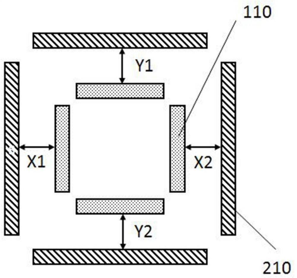
[0078] like Figure 5 As shown, the overlay marks 170 and 270 are generated at two different process levels, respectively containing four strip marks, forming a box structure. In the overlay mark 170, part of the strip mark 1701 is missing; the edge of the strip mark 1703 is not clear; in addition, the particles 1705 generated in the process are located near the overlay marks 170 and 270, which generate interference signals and affect the normality of the overlay measurement conduct.

[0079] In this embodiment, the image processing model for overlay marks described in Embodiment 1 is used to process the image data for overlay marks to solve the problem of Figure 5 problem shown. like Figure 8 As shown, the steps include the following:

[0080] For each process level, collect each overlay mark image on the wafer as the input data 2000 for overlay measurement, the input data described in this embodiment is the same as the input data in embodiment 1;

[0081] Carry out pr...

Embodiment 3

[0085] As a more preferred solution than Example 2, such as Figure 9 As shown, the difference between this embodiment and embodiment 2 is that an online model training function is added, specifically:

[0086] For each process level, collect each overlay mark image on the wafer as the input data 3000 for overlay measurement, the input data described in this embodiment is the same as the input data in embodiment 1;

[0087] Perform preprocessing on the above-mentioned input data 3000, the preprocessing described in this embodiment is the same as that in Embodiment 1;

[0088] The above-mentioned preprocessed data 3100 is input to the overlay mark image processing model 3200, and the overlay mark image processing model 3200 processes the overlay mark image through a machine learning method, such as Figure 5 As shown, the deployed overlay labeling image processing model 3200 can reconstruct the striped labeling pattern 1702 and blurred pattern 1704, and remove the pattern of p...


PUM


Abstract

The invention discloses an overlay measurement method in an integrated circuit chip manufacturing process, which comprises the following steps of: aiming at each process level of the chip manufacturing process, acquiring each piece of overlay mark image data on a wafer or acquiring overlay measurement data in a partial region on the wafer; respectively establishing machine learning models by utilizing the collected overlapping mark image data or overlapping measurement data, wherein the machine learning models comprise an overlapping mark image processing model and an overlapping measurement data prediction model; and during overlapping measurement, processing an overlapping mark image by the established overlapping mark image processing model, or predicting overlapping measurement data in other unmeasured areas on the same wafer by the established overlapping measurement data prediction model and the overlapping measurement data collected in partial areas on the wafer. According to the invention, the machine learning model is used to process or predict the data of the superposition measurement, and the stability, precision and measurement efficiency of the superposition measurement are improved.

Description

technical field [0001] The invention relates to the technical field of pattern overlay of integrated circuit chips, in particular to an overlay measurement method and system in the manufacturing process of integrated circuit chips. Background technique [0002] The manufacturing process of an integrated circuit (Integrated Circuit) chip involves multiple process levels (Layer). Each process level forms a pattern of photolithographic materials on the wafer through the photolithography process, and uses this as a template to form circuit devices and interconnection structures that meet the design specifications by using various processes such as etching, deposition, and chemical mechanical polishing. The overlay of process graphics between different process levels is very important. If the overlay error exceeds the allowable range, the circuit device and the interconnection structure will not work properly. [0003] In order to ensure the precise alignment of patterns betwee...

Claims


Application Information

Patent Timeline
IPC IPC(8): G06F30/392G06F30/398G06N20/00
CPCG06F30/392G06F30/398G06N20/00
Inventor 蒋信
Owner 普赛微科技(杭州)有限公司
Learn More