Field effect transistor, preparation method thereof and switching circuit

A field effect transistor and gallium nitride layer technology, which is applied to circuits, electrical components, and electric solid-state devices, can solve problems such as easy breakdown, unstable threshold voltage of field effect transistors, and difficulty in charge discharge.

Pending Publication Date: 2021-07-27
HUAWEI TECH CO LTD
View PDF6 Cites 4 Cited by
  • Summary
  • Abstract
  • Description
  • Claims
  • Application Information

AI Technical Summary

Problems solved by technology

However, the gate metal layer and the gate structure are generally in Schottky contact, and two back-to-back diodes are formed in the GaN field effect transistor, which makes the threshold voltage of the field effect transistor unstable due to the diffic

Method used


Image

  • Field effect transistor, preparation method thereof and switching circuit
  • Field effect transistor, preparation method thereof and switching circuit
  • Field effect transistor, preparation method thereof and switching circuit

Examples


Embodiment Construction

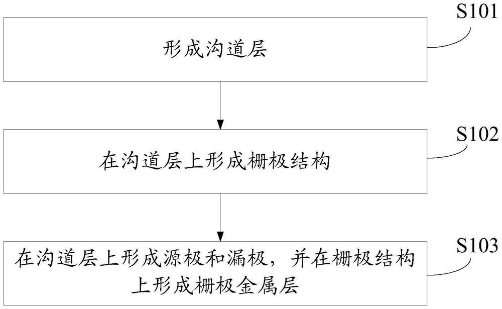
[0034]In order to make the purpose, technical solution and advantages of the application clearer, the application will be further described in detail below in conjunction with the accompanying drawings.

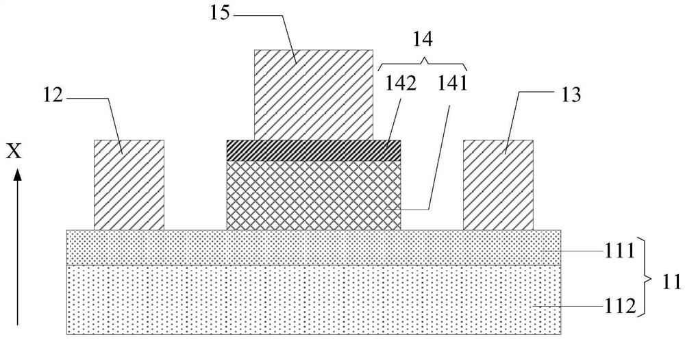
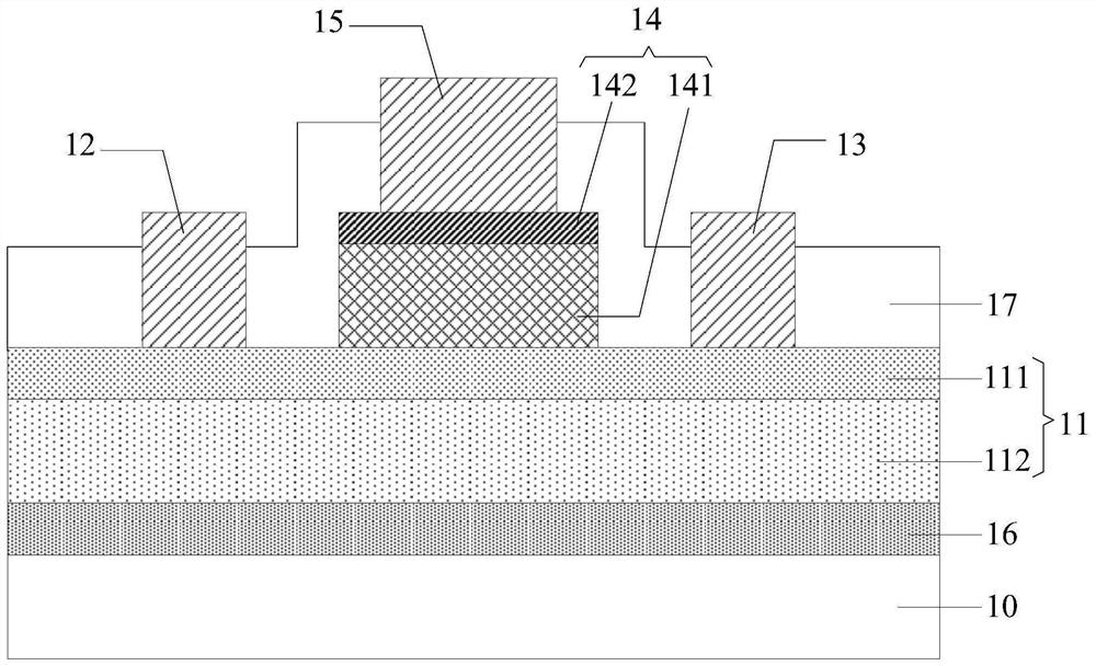
[0035] The field effect transistor provided in the embodiment of the present application is widely used as a circuit switch component in various scenarios, and the field effect transistor of GaN (gallium nitride) series material has high mobility and high chemical stability due to its material characteristics. It can be used as a higher frequency switch application, so it is widely used in high frequency circuit switches.

[0036] The GaN field effect transistor achieves the purpose of switching by controlling the on-off of the two-dimensional electron gas of the channel. GaN FETs are usually divided into two categories, one is normally-on FET, also known as depletion-type FET; the other is normally-off FET, also known as enhanced FET. However, due to the safety consideratio...


PUM

PropertyMeasurementUnit
Thicknessaaaaaaaaaa
Doping concentrationaaaaaaaaaa
Thicknessaaaaaaaaaa

Abstract

The invention provides a field effect transistor, a preparation method thereof and a switching circuit. The field effect transistor comprises a channel layer, a source electrode, a drain electrode, a gate structure and a gate metal layer, the gate structure comprises a P-type gallium nitride layer and an N-type gallium nitride layer which are stacked, so that a gate metal/pGaN Schottky diode is replaced by an nGaN/pGaN reverse biased diode, the gate voltage endurance capability of the field effect transistor can be improved, and the breakdown capability is improved. And the doping concentration of the P-type gallium nitride layer is 1 * 10 < 18 > cm <-3> to 1 * 10 < 19 > cm <-3>, so that the charge storage effect when the device works can be reduced, carriers in the pGaN layer are exhausted as much as possible, redundant charge storage is avoided, and the working threshold voltage stability of the device is improved. Ohmic contact is adopted between the gate metal layer and the gate structure, the reliability of connection between the gate metal layer and the gate structure can be improved, and therefore the reliability of the field effect transistor is improved.

Description

technical field [0001] The present application relates to the technical field of semiconductors, in particular to a field effect transistor, its preparation method and a switch circuit. Background technique [0002] Field effect transistors are widely used in various scenarios as circuit switch components, and GaN (gallium nitride)-based field effect transistors have high mobility and high chemical stability due to their material properties, and can be used as higher frequency switching applications. [0003] The GaN field effect transistor achieves the purpose of switching by controlling the on-off of the two-dimensional electron gas of the channel. GaN FETs are usually divided into two categories, one is normally-on FET, also known as depletion-type FET; the other is normally-off FET, also known as enhanced FET. However, due to the safety considerations of the power system, the switching device is generally required to be a normally-off device, and there are several ways...

Claims


Application Information

Patent Timeline
IPC IPC(8): H01L29/06H01L29/20H01L29/778H01L21/335H01L27/085
CPCH01L29/0615H01L29/2003H01L29/66462H01L29/778H01L27/085
Inventor 包琦龙蒋其梦唐高飞王汉星吉尔伯托·库拉托拉
Owner HUAWEI TECH CO LTD
Why Eureka
Try Eureka