Semiconductor device

A semiconductor and device technology, applied in the field of semiconductor devices, can solve problems such as high cost and reduced electrostatic discharge protection ability, and achieve the effects of preventing electrical breakdown, improving ESD capability, and increasing drain resistance

Pending Publication Date: 2021-07-30
SHANGHAI HUAHONG GRACE SEMICON MFG CORP
View PDF0 Cites 1 Cited by
  • Summary
  • Abstract
  • Description
  • Claims
  • Application Information

AI Technical Summary

Problems solved by technology

[0003] In the prior art, in order to overcome the problem of the decrease of electrostatic discharge protection ability brought about by the lightly doped drain (Lightly Doped Drain, LDD) structure, the electrostatic discharge ion implantation (ESD implant) technology is usually combined with the silicide baffle (Salicide Blocking (SAB) process, using SAB technology to increase the resistance of the drain region to improve the current discharge capability of the device, so that the current can flow uniformly in the silicon wafer, and the ESD device needs a SAB mask to improve the ESD protection capability of the device , while the cost of the SAB mask is relatively high, and reducing the mask can reduce the manufacturing cost, especially for the design and manufacture of nanoscale integrated circuits

Method used


Image

  • Semiconductor device

Examples


Embodiment Construction

[0024] The specific implementation manner of the present invention will be described in more detail below with reference to schematic diagrams. The advantages and features of the present invention will be more apparent from the following description. It should be noted that all the drawings are in a very simplified form and use imprecise scales, and are only used to facilitate and clearly assist the purpose of illustrating the embodiments of the present invention.

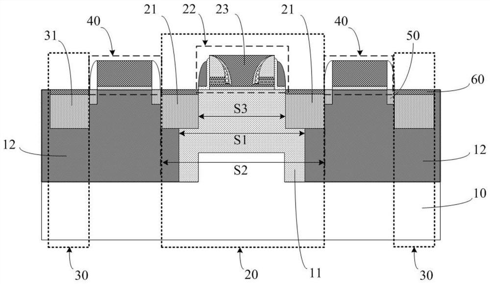
[0025] figure 1 A schematic structural diagram of a semiconductor device provided in this embodiment. This embodiment provides a semiconductor device. The ESD capability of the device is improved through the dummy structure, and the dummy can be directly formed synchronously in the manufacturing process without the need for the SAB mask in the prior art and without introducing a new process flow. structure to reduce the manufacturing cost of the device. Please refer to figure 1 , the semiconductor device includ...


PUM


Abstract

The invention provides a semiconductor device comprising a substrate having a first region and second regions, the first region being located between two adjacent second regions; two sub drain regions located in the first region of the substrate; a dummy structure positioned on the substrate between the two adjacent sub drain regions; a source region located in the second region of the substrate; a gate structure positioned on the substrate between the first region and the second regions. The ESD capacity of the device is improved through the dummy structure, an SAB photomask in the prior art is not needed, a new technological process does not need to be introduced, and the dummy structure can be directly and synchronously formed in the manufacturing process, so that the manufacturing cost of the device is reduced.

Description

technical field [0001] The invention relates to the technical field of semiconductors, in particular to a semiconductor device. Background technique [0002] As semiconductor device technology continues to enter submicron and deep submicron, the reliability of electrostatic discharge protection devices is becoming more and more important. Due to electrostatic discharge (Electro-Static-Discharge, ESD) causes discharge current to flow through the device and generates local heating or electric field concentration, electrostatic damage is prone to occur in the device, resulting in failure of the IC device; short circuit to ground at a certain terminal of the device , then a current pulse is generated at the moment of discharge, and the Joule heat generated by the large current causes the local metallization of the device to melt or the hot spots on the chip to induce secondary breakdown, etc.; when the device is not in contact with the ground, there is no direct discharge path t...

Claims


Application Information

Patent Timeline
Patent Type & Authority Applications(China)
IPC IPC(8): H01L27/02
CPCH01L27/0292
Inventor 严强生刘冲陈宏
Owner SHANGHAI HUAHONG GRACE SEMICON MFG CORP
Why Eureka
Try Eureka