

Semiconductor package and method for fabricating same
A packaging and semiconductor technology, applied in semiconductor/solid-state device manufacturing, semiconductor devices, semiconductor/solid-state device components, etc., can solve problems such as increasing the density of delayed products
- Summary
- Abstract
- Description
- Claims
- Application Information
AI Technical Summary
Problems solved by technology
Method used
Image

Examples
Embodiment Construction
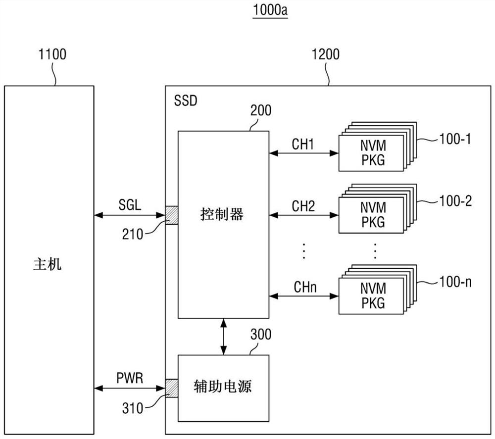
[0021] figure 1 is an exemplary block diagram illustrating a memory system including a semiconductor package according to an exemplary embodiment of the inventive concept.
[0022] refer to figure 1 , the storage system 1000a includes a host 1100 (for example, a host device) and a storage device 1200 .
[0023] According to some embodiments, the memory device 1200 includes a plurality of non-volatile memory packages (NVM PKG) 100-1, 100-2 to 100-n and a controller 200 (eg, a control circuit). A plurality of nonvolatile memory packages 100 - 1 , 100 - 2 to 100 - n may be used as storage media of the storage device 1200 . Each of the plurality of nonvolatile memory packages 100-1, 100-2 to 100-n may include a plurality of nonvolatile memory chips. In an exemplary embodiment, each of the plurality of nonvolatile memory chips includes a flash memory device.
[0024] The controller 200 may be connected to each of the plurality of nonvolatile memory packages 100-1, 100-2 to 100-...
PUM
 Abstract
Description
Claims
Application Information