
Method for improving poor back sealing pinholes of large-diameter semiconductor silicon wafer

A semiconductor and large-diameter technology, applied in semiconductor/solid-state device manufacturing, chemical instruments and methods, crystal growth, etc., can solve problems such as poor back-sealing pinholes and silicon chip pinholes, and improve back-sealing pinhole defects , reduce the surface impurities of incoming materials, and improve the effect of equipment maintenance methods

Pending Publication Date: 2021-08-13
ZHONGHUAN ADVANCED SEMICON MATERIALS CO LTD
View PDF5 Cites 0 Cited by
  • Summary
  • Abstract
  • Description
  • Claims
  • Application Information

AI Technical Summary

Problems solved by technology

[0004] The object of the present invention is to provide a method for improving the bad pinholes in the back seal of large-diameter semiconductor silicon wafers, so as to solve some problems in the incoming materials, equipment exhaust and cleaning and maintenance proposed in the above-mentioned background technology, which eventually lead to back seal failure. The pinhole defect is high, and when the silicon dioxide film is prepared by the normal pressure equipment, due to the dust falling of the equipment itself and the impurities in the operator or the environment falling on the product, the pinhole defect will be formed on the surface of the silicon wafer after coating question

Method used

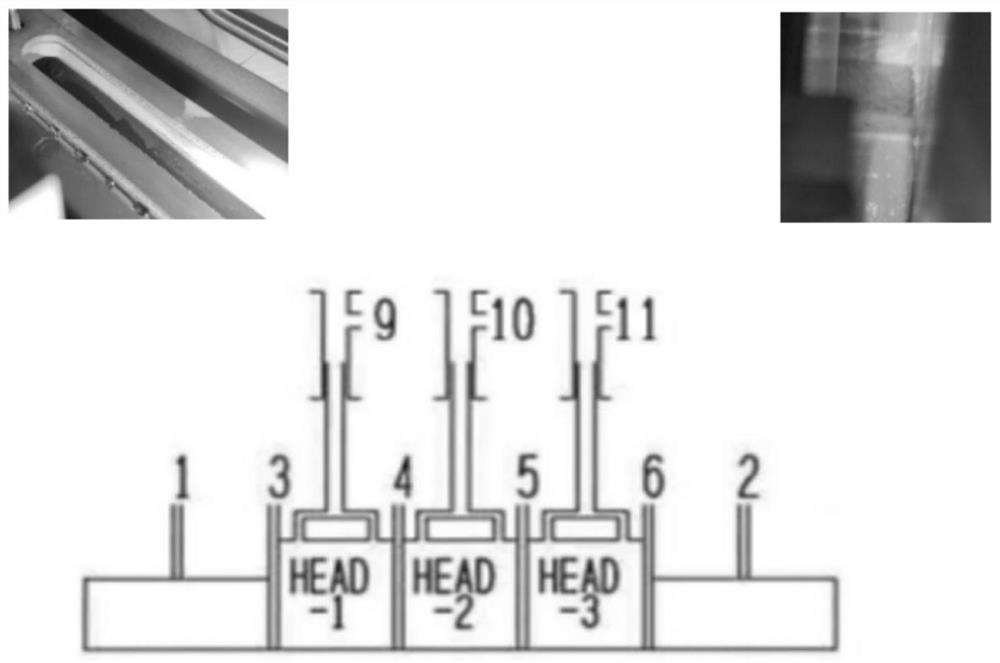

Image

  • Method for improving poor back sealing pinholes of large-diameter semiconductor silicon wafer
  • Method for improving poor back sealing pinholes of large-diameter semiconductor silicon wafer
  • Method for improving poor back sealing pinholes of large-diameter semiconductor silicon wafer

Examples


Embodiment 1

[0029] The experimental method of the present embodiment comprises the following steps:

[0030] Pre-LTO cleaning is carried out through the Pre-cvd cleaning machine, and the secondary distribution personnel are linked to increase the frequency conversion fan with harmful exhaust air. After the harmful exhaust air of the equipment is stabilized, the general exhaust air is adjusted to finally ensure the pressure balance of the equipment cavity, and the frequency conversion exhaust air can be added. Stabilize the fluctuation of harmful exhaust air, prevent the dust from falling on the silicon wafer due to the fluctuation of exhaust air during the film forming process, and form pinholes. During the filming process, it enters the equipment cavity and falls on the silicon wafer to form a pinhole defect. The linkage production arranges machine cleaning and feeding, and the full inspection is carried out through fluorescent lamp visual inspection.

[0031] In the present embodiment, ...

Embodiment 2

[0044] The difference from Embodiment 1 is that:

[0045] The experimental method of the present embodiment comprises the following steps:

[0046] S1. The first machine: use the Pre-cvd cleaning machine to perform pre-LTO cleaning, link the secondary distribution personnel to increase the frequency conversion fan for harmful exhaust air, adjust the general exhaust air after stabilizing the harmful exhaust air of the equipment, and finally ensure the pressure balance of the equipment cavity. Increasing frequency conversion exhaust air can stabilize the fluctuation of harmful exhaust air, and prevent the dust from falling on the silicon wafer due to the fluctuation of exhaust air during the film forming process, resulting in poor pinholes. Before film formation or during film formation, it enters the equipment cavity and falls on the silicon wafer to form pinholes.

[0047] S2. Next method: Compile the instruction manual for equipment nozzle cleaning and maintenance. According...

Embodiment 3

[0061] The difference with embodiment one and embodiment two is characterized in that:

[0062] The experimental method of the present embodiment comprises the following steps:

[0063] S1. The first machine: use the Pre-cvd cleaning machine to perform pre-LTO cleaning, link the secondary distribution personnel to increase the frequency conversion fan for harmful exhaust air, adjust the general exhaust air after stabilizing the harmful exhaust air of the equipment, and finally ensure the pressure balance of the equipment cavity. Increasing frequency conversion exhaust air can stabilize the fluctuation of harmful exhaust air, and prevent the dust from falling on the silicon wafer due to the fluctuation of exhaust air during the film forming process, resulting in poor pinholes. Before film formation or during film formation, it enters the equipment cavity and falls on the silicon wafer to form pinholes.

[0064] S2. Next method: Compile the instruction manual for equipment nozz...


PUM


Abstract

The invention discloses a method for improving poor back sealing pinholes of a large-diameter semiconductor silicon wafer. The experiment method comprises the following steps that S1, firstly, a machine stage is carried out, specifically, LTO pre-cleaning is performed through a Pre-cvd cleaning machine, a frequency conversion fan is added for harmful air exhaust through linkage with secondary distribution personnel, general air exhaust is adjusted after stabilizing the harmful air exhaust of equipment, finally the pressure balance of an equipment cavity is guaranteed, frequency conversion air exhaust is added to stabilize fluctuation of harmful air exhaust, the phenomenon that in a film forming process, due to the fact that air exhaust fluctuates, dust falls on a silicon wafer, and poor pinholes are formed is avoided, and then the situation that outside dust enters the equipment cavity before film forming or in the film forming process of the silicon wafer, and falls on the silicon wafer, and poor pinholes are formed is avoided by stabilizing cavity pressure balance; and S2, secondly, a law stage is carried out, specifically, a cleaning and maintenance operation instruction book of an equipment nozzle is compiled, and according to the principle that when the accumulated film thickness of the equipment nozzle reaches a certain thickness, the exhaust pressure cannot suck the dust in time, corners where the dust is prone to accumulation of the equipment nozzle are found, and a brush matched with cleaning is purchased.

Description

technical field [0001] The invention relates to the technical field of improving the appearance of an 8-inch back-sealing sheet, in particular to a method for improving the bad pinholes in the back-sealing of a large-diameter semiconductor silicon wafer. Background technique [0002] Monocrystalline silicon wafers are mostly used as substrate materials for manufacturing integrated circuits. The surface quality of silicon wafers can directly affect customers' judgment and utilization of products. As the size of silicon wafers increases, there are higher requirements for the appearance of silicon wafers. , and can better reflect the processing level of silicon wafers. The back-sealing process of 8-inch silicon wafers is: cleaning before back-sealing → back-sealing. When the cumulative film thickness of the nozzles of the back-sealing equipment reaches a certain thickness, dust will be generated due to insufficient exhaust pressure. Dropped on the silicon wafer, poor pinholes a...

Claims


Application Information

Patent Timeline
Patent Type & Authority Applications(China)
IPC IPC(8): C23C16/02C23C16/40C23C16/44C30B29/06C30B33/00H01L21/02
CPCC23C16/0227C23C16/402C23C16/4401C23C16/4412C30B33/00C30B29/06H01L21/02054
Inventor 王昊宇江笠孙晨光王彦君
Owner ZHONGHUAN ADVANCED SEMICON MATERIALS CO LTD
Learn More