Chip on film, display module and display device

A chip-on-chip film and display module technology, which is applied to printed circuit components, circuit substrate materials, metal pattern materials, etc., to achieve the effects of improving quality, preventing oxidation, and simplifying process steps

Active Publication Date: 2021-08-13
WUHAN TIANMA MICRO ELECTRONICS CO LTD
View PDF4 Cites 3 Cited by
  • Summary
  • Abstract
  • Description
  • Claims
  • Application Information

AI Technical Summary

Problems solved by technology

[0005] Embodiments of the present invention provide a chip-on-chip film, a display module, and a display device to solve the problems existing in the existing chip-on-chip film, improve the quality of the display module, and improve production efficiency

Method used


Image

  • Chip on film, display module and display device
  • Chip on film, display module and display device
  • Chip on film, display module and display device

Examples


Embodiment Construction

[0023] The present invention will be further described in detail below in conjunction with the accompanying drawings and embodiments. It should be understood that the specific embodiments described here are only used to explain the present invention, but not to limit the present invention. In addition, it should be noted that, for the convenience of description, only some but not all structures related to the present invention are shown in the accompanying drawings, and the shapes and sizes of each structure in the accompanying drawings do not reflect their true proportions, and the purpose is only to illustrate the present invention. Invention content.

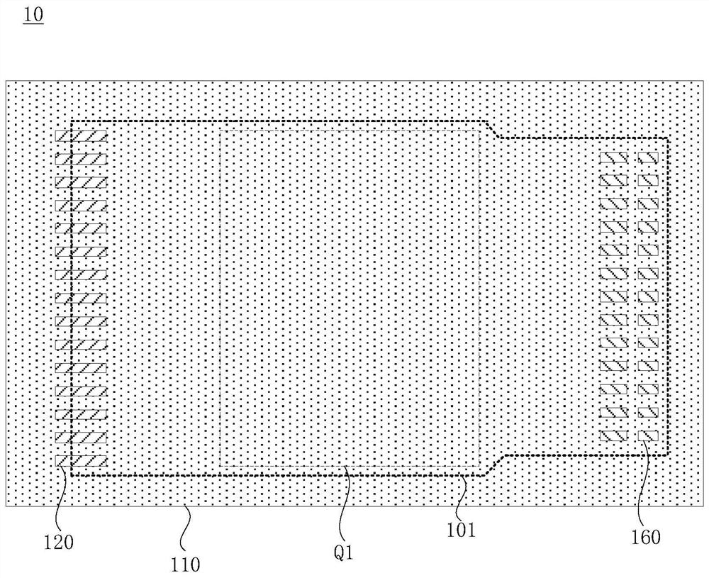
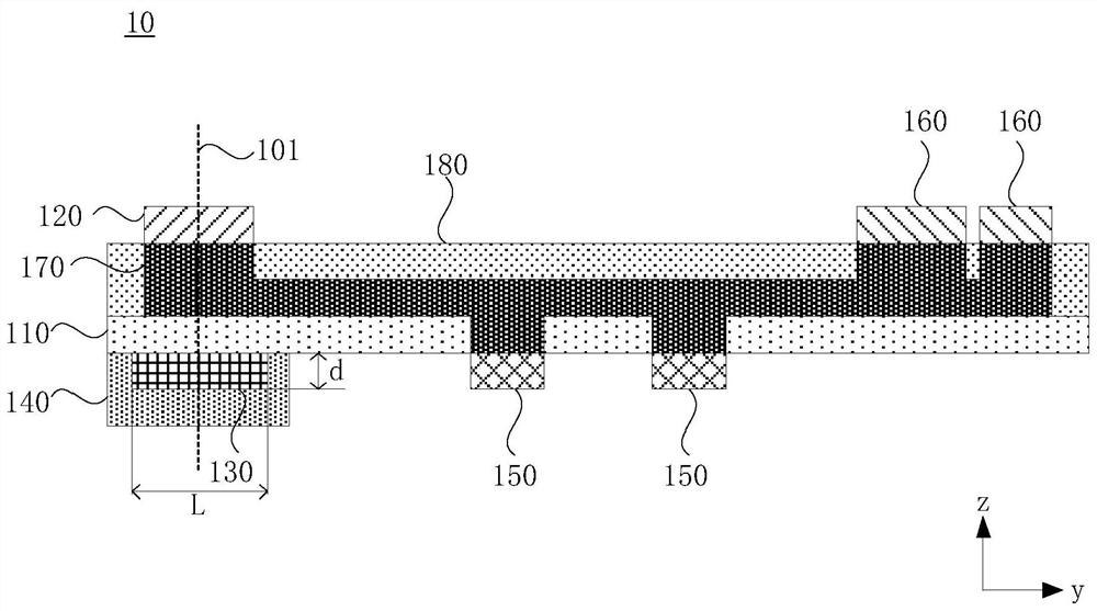
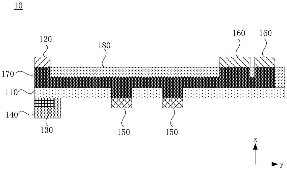
[0024] figure 1 It is a top view structure diagram of a chip-on-chip film provided by an embodiment of the present invention before it is punched out, figure 2 It is a schematic cross-sectional structure diagram of a chip-on-chip film provided by an embodiment of the present invention before it is punched, see figure 1 an...


PUM

PropertyMeasurementUnit
thicknessaaaaaaaaaa
lengthaaaaaaaaaa

Abstract

The embodiment of the invention discloses a chip on film, a display module and a display device. The chip on film comprises a flexible substrate, a plurality of first binding terminals located on one side of the flexible substrate and a first protection layer located on the side, away from the first binding terminals, of the flexible substrate. The first binding terminals are used for being correspondingly bound with electrodes of a binding area of the display panel. The vertical projection of the first protection layer on the flexible substrate and the vertical projection of the first binding terminals on the flexible substrate are overlapped with the cutting line at the same position of the chip on film, and the first protection layer is heated and melted. According to the technical scheme, the problems existing in an existing chip on film can be solved, the quality of the display module is improved, and the production efficiency is improved.

Description

technical field [0001] Embodiments of the present invention relate to the field of display technology, and in particular, to a chip-on-film, a display module, and a display device. Background technique [0002] Chip On Film (COF) is a soft additional circuit board for unpackaged chips. It is mainly used to connect display panels, driver chips and printed circuit boards during the bonding stage of the display device manufacturing process. Form a pathway. [0003] In order to adapt to the development trend of narrow borders, the size of the electrodes in the bonding area of ​​the display panel is usually very small. Therefore, the chip-on-film needs to be punched first to obtain the required specifications of the chip-on-film, and at the same time reduce the bonding terminals on the chip-on-film (gold finger) size, and then bind. [0004] However, the existing chip-on-film structure has the following problems after punching and bonding. For example, after punching off the re...

Claims


Application Information

Patent Timeline
Patent Type & Authority Applications(China)
IPC IPC(8): H05K1/05H05K1/09
CPCH05K1/09H05K1/05
Inventor 鲍垚
Owner WUHAN TIANMA MICRO ELECTRONICS CO LTD
Why Eureka
Try Eureka