

Wafer grinding equipment for research and development of high-side NMOSFET driver chip
A driver and chip technology, applied in the direction of grinding/polishing equipment, grinding machine tools, grinding tools, etc., can solve the problems of large limitations, edge chipping, fragmentation, increased time, etc., and achieve a wide range of applications and good stability of the wafer Effect
- Summary
- Abstract
- Description
- Claims
- Application Information
AI Technical Summary
Problems solved by technology
Method used
Image

Examples
Embodiment 1
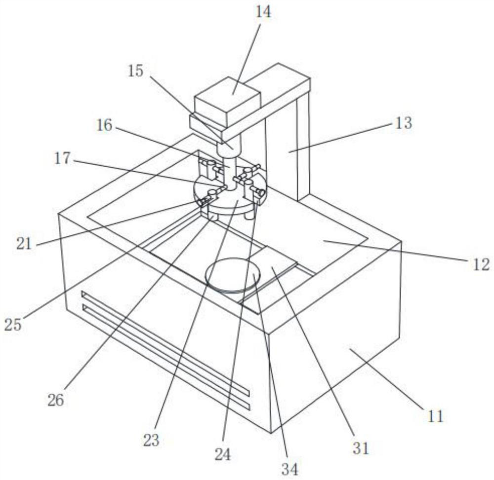
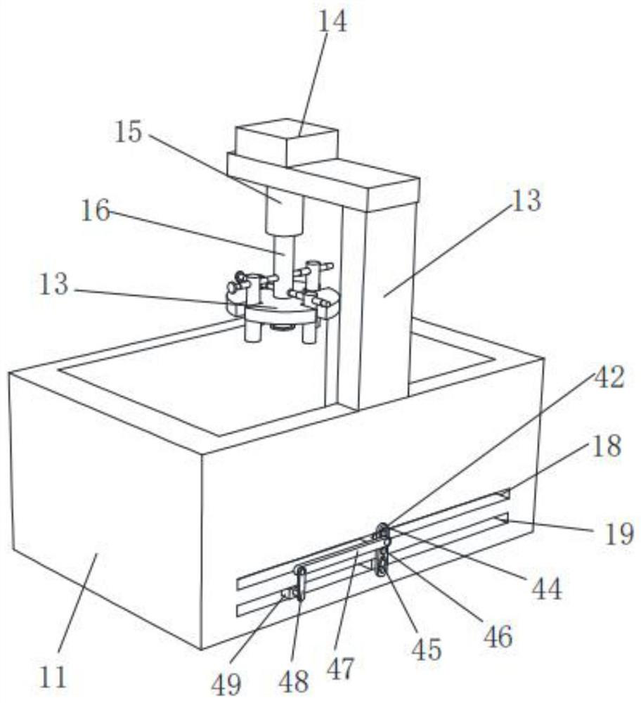
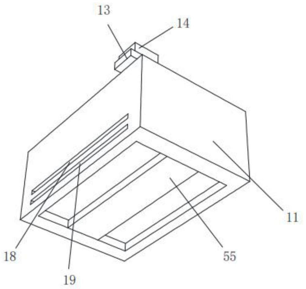
[0034] Example 1, please refer to figure 1 , Figure 7 and Figure 8 , the present invention provides a technical scheme of wafer grinding equipment for research and development of high-side NMOSFET driver chips: including a workbench 11, a rectangular groove 12 is opened at the center of the end of the workbench 11, and a connecting rod 13 is fixedly installed on the side wall of the workbench 11, The end of the connecting rod 13 is fixed with the first motor 14, the end of the first motor 14 is fixed with the column sleeve 15, and the side of the column sleeve 15 away from the first motor 14 is fixed with the hydraulic rod 16, and the hydraulic rod 16 runs through the equipment Adjustment column 17 is arranged, and the side wall of workbench 11 is provided with first bar-shaped groove 18 and second bar-shaped groove 19, and second bar-shaped groove 19 is positioned at first bar-shaped groove 18 lower ends, and second bar-shaped groove 19 interior is provided with Same stru...
Embodiment 2
[0038] Example 2, please refer to Figure 6 and Figure 9 , On the basis of Embodiment 1, the surface of the adjustment column 17 is covered with an adjustment mechanism.
[0039] The adjustment mechanism includes a threaded sleeve 21. Two threaded sleeves 21 are arranged symmetrically with the midpoint of the adjustment column 17 as the center point, and the threads on the surfaces of the two threaded sleeves 21 are in opposite directions. Rotary cap 22 is fixedly installed on the upper part, and a turntable 23 is fixedly installed on the side of the hydraulic rod 16 away from the column sleeve 15. The side wall of the turntable 23 is evenly mixed and equidistantly provided with a card slot 24, and a fixed column 25 is arranged inside the card slot 24, and the fixed column The surface of 25 is covered with a grinding sleeve 26, the side of the turntable 23 away from the hydraulic rod 16 is fixedly installed with an extrusion column 27, and the end of the extrusion column 27 ...
Embodiment 3
[0041] Embodiment three, please refer to figure 2 , image 3 , Figure 4 and Figure 5 , On the basis of Embodiment 1, a shaking mechanism is provided inside the first bar-shaped groove 18 .
[0042] The rocking mechanism comprises a slide bar 41, the slide bar 41 is arranged inside the first strip groove 18, the side wall of the end of the slide bar 41 is fixedly equipped with a slide block 42, and the end of the slide block 42 is fixedly equipped with a first movable column 43, and the first movable column 43 is fixedly installed at the end of the slide bar 42. Movable column 43 surface activities are provided with arc bar 44, and arc bar 44 sidewalls are provided with arc groove 45, and first movable column 43 is located in the arc groove 45 inside that is positioned at upper end, and arc bar 44 side walls middle part There is a central column 46 inside, and the opposite side of the central column 46 is fixedly connected to the workbench 11. The surface of the first mov...
PUM
 Abstract
Description
Claims
Application Information