Display panel and manufacturing method thereof

A technology for a display panel and a manufacturing method, which is applied in the manufacturing of semiconductor/solid-state devices, electrical components, and electrical solid-state devices, etc., can solve problems such as mutual crosstalk, and achieve the effect of ensuring normal operation.

Pending Publication Date: 2021-08-24
WUHAN CHINA STAR OPTOELECTRONICS SEMICON DISPLAY TECH CO LTD
View PDF5 Cites 0 Cited by
  • Summary
  • Abstract
  • Description
  • Claims
  • Application Information

AI Technical Summary

Problems solved by technology

[0004] As the thickness of the TFE structure decreases, the capacitance between the metal wiring in the Touch Sensor and th

Method used


Image

  • Display panel and manufacturing method thereof
  • Display panel and manufacturing method thereof
  • Display panel and manufacturing method thereof

Examples


Example Embodiment

[0041] Embodiment one,

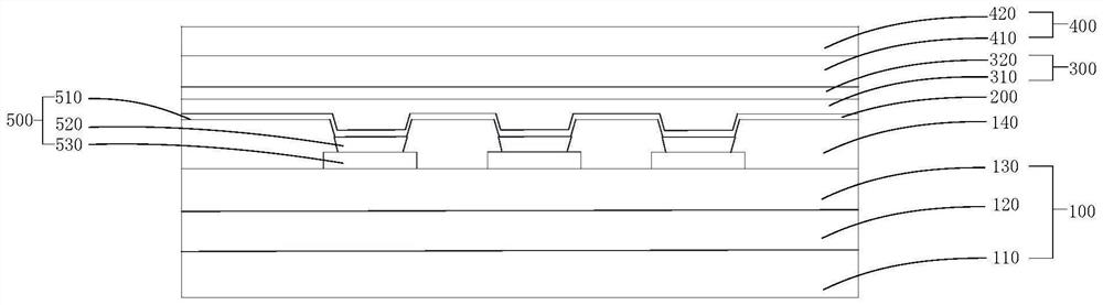
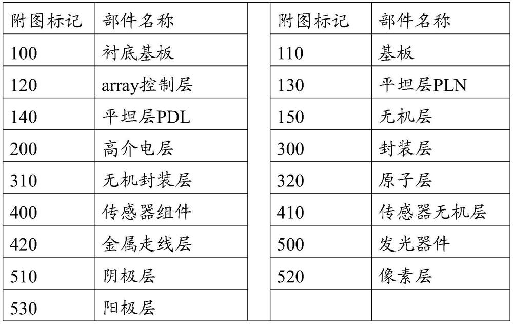
[0042] The first embodiment of the present application discloses a display panel, which includes from bottom to top: a base substrate 100, a light emitting device 500, an encapsulation layer 300, and a sensor assembly 400, and the encapsulation layer 300 passes between the light emitting device 500 and the sensor assembly 400 Separated, wherein both the light emitting device 500 and the sensor component 400 are energized to work, and when the encapsulation layer 300 is thin, the capacitance of the encapsulation layer 300 is low, and mutual crosstalk between the light emitting device 500 and the sensor component 400 is prone to occur, resulting in abnormal light emission or sensor failure occurs.

[0043] In view of this, the display panel in this embodiment further includes: a high dielectric layer 200, the high dielectric layer 200 is arranged between the encapsulation layer 300 and the light emitting device 500, the high dielectric layer 200 has a re...

Example Embodiment

[0048] Embodiment two,

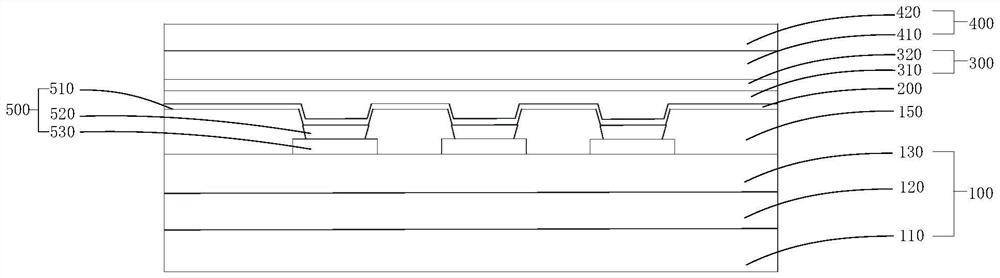
[0049] The second embodiment of the present application relates to a display panel, which is generally the same as the display panel in the first embodiment. The control layer 120, the flat layer PLN130 disposed on the array control layer 120, and the inorganic layer 150 disposed on the flat layer PLN130. In this embodiment, the flat layer PDL140 in the first embodiment is replaced by the inorganic layer 150. The inorganic layer 150 It is disposed on the flat layer PLN130 , and the light emitting device 500 is disposed in the inorganic layer 150 . The inorganic layer 150 can further strengthen the water and oxygen barrier capability of the side of the pixel layer 520 to protect the light emitting device 500 .

Example Embodiment

[0050] Embodiment three,

[0051] The third embodiment of the present application discloses a method for manufacturing a display substrate, which can be used to manufacture the display substrate in the first embodiment or the second embodiment, including the following steps:

[0052] A base substrate is provided; the base substrate includes: a substrate, an array control layer disposed on the substrate, a flat layer PLN disposed on the array control layer, and a flat layer PDL disposed on the flat layer PLN; wherein the flat layer can be formed by the PDL replaced by an inorganic layer.

[0053] disposing a light emitting device on the substrate;

[0054] Deposit a high dielectric layer on the light-emitting component; the high dielectric layer is Al 2 o 3 Film layer, ZrO 2 film or HfO 2 One of the membrane layers. In this embodiment, the PVD method can be used to deposit a certain thickness of Al 2 o 3 , forming Al 2 o 3 film layer, deposited directly on the cathode...


PUM


Abstract

The embodiment of the invention discloses a display panel and a manufacturing method thereof. The display panel comprises: a substrate; a light-emitting device which is arranged on the substrate; an encapsulation layer; and a light-emitting device which is arranged on the packaging layer, wherein the high dielectric layer is arranged between the light-emitting device and the packaging layer, the sensor assembly is arranged on the packaging layer, and the sensor assembly and the light-emitting device are separated through the high dielectric layer and the packaging layer. According to the embodiment of the invention, the scheme that the light-emitting device and the sensor assembly are separated through the high dielectric layer and the packaging layer is adopted, the high capacitance value of the high dielectric layer can avoid the situation of mutual crosstalk between the light-emitting device and the sensor assembly, and normal work of the light-emitting device and the sensor assembly is guaranteed.

Description

technical field [0001] The present application relates to the display field, in particular to a display panel and a manufacturing method thereof. Background technique [0002] OLED (Organic Light Emitting Diode, Organic Light Emitting Diode) display technology is an emerging flat panel display technology. Due to the advantages of wide viewing angle, self-illumination, and ultra-fast response, OLED technology is widely used in the display field. [0003] In a light-emitting device of a top-emitting OLED, the main structure includes a substrate, a metal anode arranged on the substrate, a light-emitting functional layer arranged on the metal anode, and a metal cathode arranged on the light-emitting functional layer. However, the luminescent material is very sensitive to water and oxygen, and TFE (Thin Film Encapsulation) film packaging technology is usually used to isolate the luminescent material from water and oxygen. With the advancement of technology, in order to reduce c...

Claims


Application Information

Patent Timeline
IPC IPC(8): H01L51/52H01L27/32H01L51/56
CPCH10K59/40H10K59/126H10K50/84H10K59/1201H10K71/00
Inventor 许喆
Owner WUHAN CHINA STAR OPTOELECTRONICS SEMICON DISPLAY TECH CO LTD
Why Eureka
Try Eureka