
Design method and welding method based on inter-board vertical interconnection printed board assembly

A design method and technology of printed boards, applied in the direction of printed circuit manufacturing, printed circuit making wiring diagrams, electrical components, etc., can solve the problem of inter-board surface mount Signal transmission stability and other issues to achieve the effect of improving placement efficiency, ensuring welding quality and solving warping deformation

Active Publication Date: 2021-08-24
SOUTHWEST CHINA RES INST OF ELECTRONICS EQUIP
View PDF12 Cites 5 Cited by
  • Summary
  • Abstract
  • Description
  • Claims
  • Application Information

AI Technical Summary

Problems solved by technology

According to the traditional printed board assembly design method and the traditional SMT welding method to design and manufacture this printed board assembly, it is easy to have the position deviation of the surface mount connector after welding, the connector tilt, the floating height, the warping deformation of the printed board, etc. problems, which in turn affect the mating of surface mount connectors between boards, reduce the reliability of vertical interconnection between boards, and affect the stability of electrical signal transmission

Method used


Image

  • Design method and welding method based on inter-board vertical interconnection printed board assembly
  • Design method and welding method based on inter-board vertical interconnection printed board assembly
  • Design method and welding method based on inter-board vertical interconnection printed board assembly

Examples


Embodiment Construction

[0067] In order to make the purpose, technical solutions and advantages of the embodiments of the present invention clearer, the technical solutions in the embodiments of the present invention will be clearly and completely described below in conjunction with the drawings in the embodiments of the present invention. Obviously, the described embodiments It is a part of embodiments of the present invention, but not all embodiments. The components of the embodiments of the invention generally described and illustrated in the figures herein may be arranged and designed in a variety of different configurations.

[0068] Accordingly, the following detailed description of the embodiments of the invention provided in the accompanying drawings is not intended to limit the scope of the claimed invention, but merely represents selected embodiments of the invention. Based on the embodiments of the present invention, all other embodiments obtained by persons of ordinary skill in the art wi...


PUM

PropertyMeasurementUnit
Thermal expansion coefficientaaaaaaaaaa
Glass transition temperatureaaaaaaaaaa

Abstract

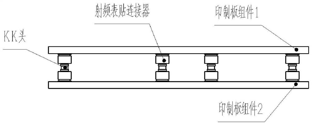
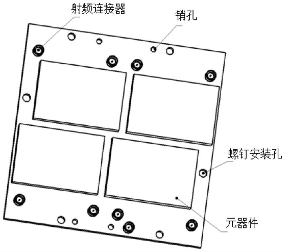
The invention relates to the field of electronic equipment, and discloses a design method and a welding method of a printed board assembly based on inter-board vertical interconnection, and the method carries out the special design of a printed board bonding pad of a surface-mounted connector and an opening of a screen printed by soldering paste, thereby achieving the self-positioning of the surface-mounted connector. A printed board anti-deformation design and an anti-deformation welding clamp are adopted to control buckling deformation in the processing and welding processes of the printed board, and accurate positioning and reliable welding of the surface-mounted connector on the printed board assembly based on inter-board vertical interconnection are achieved. According to the design method and the welding method of the printed board assembly based on the vertical interconnection between the boards, the problems that the position of the surface-mounted connector on the printed board assembly is deviated, the connector is inclined and floated, and the printed board is warped and deformed are solved, so that the realizability and the reliability of the vertical interconnection between the boards are improved.

Description

technical field [0001] The invention relates to the field of electronic equipment, in particular to the field of electrical interconnection of printed board components, and specifically designs a design method and a welding method based on vertical interconnection of printed board components between boards. Background technique [0002] Low-frequency and high-frequency signal transmission between printed board components is generally connected through cable components, through-hole plug-in connectors or insulators. However, as the number of vertically interconnected signals between printed board components increases, the traditional vertically interconnected structure has problems such as large volume, complicated assembly, and high cost. In this case, the structure of vertical interconnection between boards using surface mount connectors came into being. This multi-layer vertical interconnection structure has the advantages of small size, high interconnection density, cabl...

Claims


Application Information

Patent Timeline
IPC IPC(8): H05K3/00H05K3/34
CPCH05K3/00H05K3/0002H05K3/341
Inventor 张涛胡雅婷赵少伟何国华李杨杨非曹洪志王宇陈雨黄福清向华
Owner SOUTHWEST CHINA RES INST OF ELECTRONICS EQUIP
Learn More