Glue spraying equipment for semiconductor photoetching processing

A lithography and semiconductor technology, applied in opto-mechanical equipment, photo-engraving process coating equipment, optics, etc., can solve the problems of slow efficiency, affecting the efficiency of wafer finished products, and long operation cycle.

Inactive Publication Date: 2021-09-10
深圳恩必德电子科技有限公司
View PDF0 Cites 1 Cited by
  • Summary
  • Abstract
  • Description
  • Claims
  • Application Information

AI Technical Summary

Problems solved by technology

[0003] However, during the spin coating process of the existing glue spraying equipment, only a single concentrated nozzle sprays the glue and drives the wafer to rotate, so that the glue can be evenly covered on the wafer under the action of centrifugal force. The cycle is long, the efficiency is slow, and the phot...

Method used


Image

  • Glue spraying equipment for semiconductor photoetching processing
  • Glue spraying equipment for semiconductor photoetching processing
  • Glue spraying equipment for semiconductor photoetching processing

Examples


Embodiment Construction

[0025] The following will clearly and completely describe the technical solutions in the embodiments of the present invention with reference to the accompanying drawings in the embodiments of the present invention. Obviously, the described embodiments are only some, not all, embodiments of the present invention. Based on the embodiments of the present invention, all other embodiments obtained by persons of ordinary skill in the art without making creative efforts belong to the protection scope of the present invention.

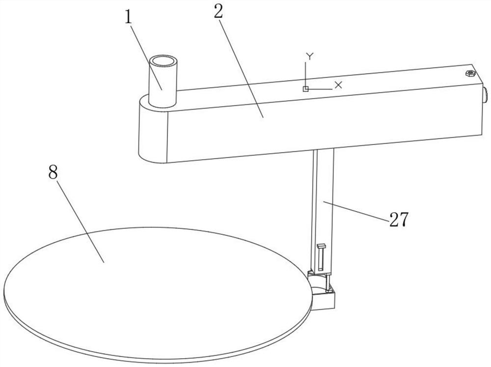
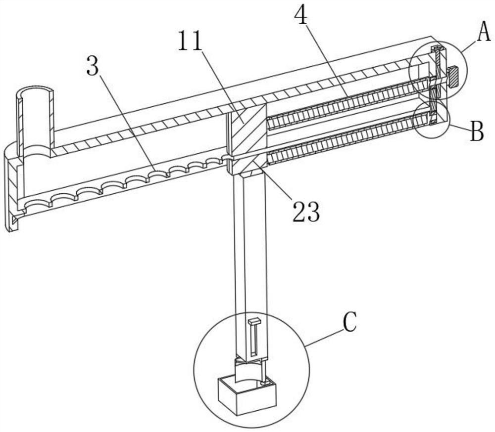
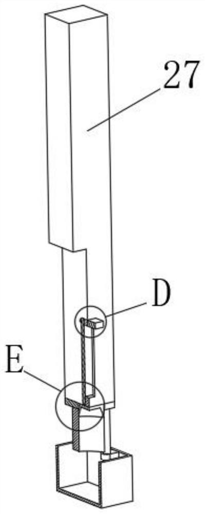
[0026] see Figure 1-9 , the present invention provides a technical solution: a glue spraying equipment for semiconductor photolithography, comprising a glue inlet 1 and a nozzle tube 2 fixedly installed at the bottom of the glue inlet 1, the bottom of the nozzle tube 2 is provided with a plurality of Glue spray port 3, the inside of the nozzle pipe 2 is provided with an anti-blocking seal 4 that adjusts the number of glue spray ports 3; a stopper 5 is provide...


PUM


Abstract

The invention discloses glue spraying equipment for semiconductor photoetching processing. The equipment comprises a glue inlet and a nozzle pipe fixedly mounted at the bottom of the glue inlet; the bottom of the nozzle pipe is provided with a plurality of glue spraying openings; and the nozzle pipe is internally provided with an anti-blocking sealing element for adjusting the number of the glue spraying openings; a limiting piece is arranged above the end part of the anti-blocking sealing element;and the lower part of the anti-blocking sealing element is connected with an auxiliary device through a connecting piece; the side surface of the auxiliary device is provided with a discharging device to deal with excess sprayed glue outside a wafer; and a material collection device is arranged below the discharging device. According to the glue spraying equipment for the semiconductor photoetching processing, the number of the glue spraying openings in the nozzle pipe can be adjusted through the anti-blocking sealing element and the auxiliary device according to the outer diameter of the wafer; a positioning scraper on the auxiliary device can remove redundant sprayed glue on the outer side of the wafer while performing positioning, so that the glue spraying efficiency of the surface of the wafer is improved, edge exposure of the wafer in the subsequent process can be avoided, and the finished product efficiency of the wafer is effectively improved.

Description

technical field [0001] The invention relates to the technical field of semiconductors, in particular to glue spraying equipment for semiconductor photolithography processing. Background technique [0002] Photolithography is one of the important process methods in the semiconductor manufacturing process, which usually includes the following steps: forming a photoresist layer on the semiconductor wafer; selectively exposing the photoresist layer, and making the exposed light through a developing step The resist layer further forms a photoresist pattern, and this step is also called patterning of the photoresist layer; using the patterned photoresist layer as a mask, the semiconductor wafer is etched; After etching, the photoresist layer is ashed to remove the photoresist layer, and the photoresist layer can be formed by spray coating or spin coating. [0003] However, during the spin coating process of the existing glue spraying equipment, only a single concentrated nozzle s...

Claims


Application Information

Patent Timeline
IPC IPC(8): G03F7/16
CPCG03F7/162G03F7/168
Inventor 罗兵甲
Owner 深圳恩必德电子科技有限公司
Why Eureka
Try Eureka