Nano-porous structure deep ultraviolet LED device with n-AlGaN layer and manufacturing method of nano-porous structure deep ultraviolet LED device

A LED device, nanoporous technology, applied in nanotechnology, semiconductor devices, electrical components, etc., can solve the problems of enhanced light extraction efficiency, no clear distinction, loss of total internal reflection of deep ultraviolet light, etc.

Pending Publication Date: 2021-09-10
XI AN JIAOTONG UNIV
View PDF11 Cites 0 Cited by
  • Summary
  • Abstract
  • Description
  • Claims
  • Application Information

AI Technical Summary

Problems solved by technology

[0003] However, after years of research, there are still problems in the research of deep ultraviolet LEDs: so far, deep ultraviolet LEDs have not achieved a large external quantum efficiency, mainly due to low light extraction efficiency, mainly including the absorption of ultraviolet light by the p-contact layer , the total internal reflection (TIR) ​​loss of deep ultraviolet light in the multilayer structure, and the unique optical polarization characteristi

Method used


Image

  • Nano-porous structure deep ultraviolet LED device with n-AlGaN layer and manufacturing method of nano-porous structure deep ultraviolet LED device
  • Nano-porous structure deep ultraviolet LED device with n-AlGaN layer and manufacturing method of nano-porous structure deep ultraviolet LED device
  • Nano-porous structure deep ultraviolet LED device with n-AlGaN layer and manufacturing method of nano-porous structure deep ultraviolet LED device

Examples


Embodiment Construction

[0036] In order to enable those skilled in the art to better understand the solutions of the present invention, the following will clearly and completely describe the technical solutions in the embodiments of the present invention in conjunction with the drawings in the embodiments of the present invention. Obviously, the described embodiments are only The embodiments are a part of the present invention, not all embodiments, and are not intended to limit the scope of the present invention. Also, in the following description, descriptions of well-known structures and techniques are omitted to avoid unnecessarily obscuring the concepts disclosed in the present invention. Based on the embodiments of the present invention, all other embodiments obtained by persons of ordinary skill in the art without making creative efforts shall fall within the protection scope of the present invention.

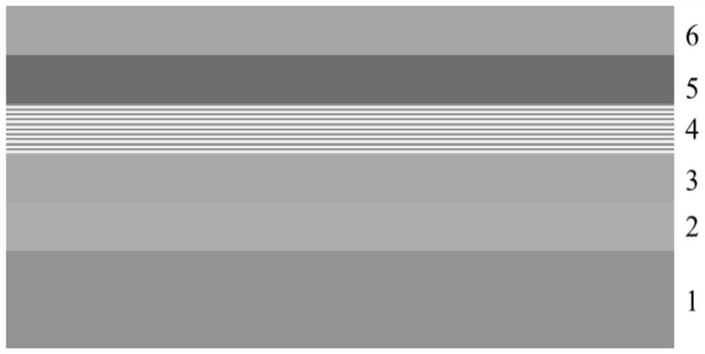
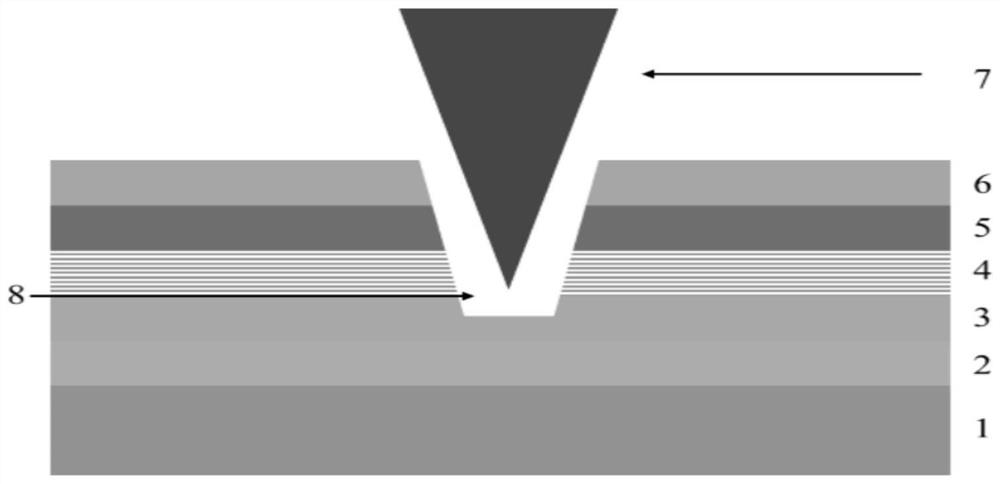
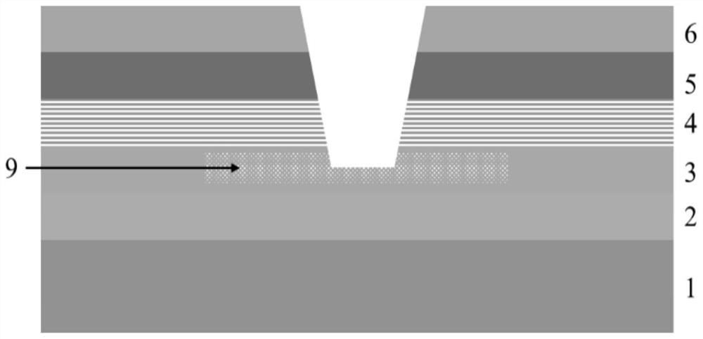
[0037] The schematic diagrams of the structures according to the disclosed embodiments of th...


PUM


Abstract

The invention discloses a nano-porous structure deep ultraviolet LED device with an n-AlGaN layer and a manufacturing method of the nano-porous structure deep ultraviolet LED device. The nano-porous structure deep ultraviolet LED device comprises a sapphire substrate, an AlN layer, an n-AlGaN layer, a multi-quantum well layer, a p-AlGaN layer, a p-GaN layer, a p electrode and an n electrode, wherein the n-AlGaN layer and the AlN layer are sequentially arranged on the sapphire substrate from top to bottom, the n electrode and the multi-quantum well layer are arranged on the n-AlGaN layer, the p electrode 10, the p-GaN layer, the p-AlGaN layer and the multi-quantum well layer are sequentially arranged on the n-AlGaN layer from top to bottom, and a nano-porous structure is arranged in the n-AlGaN layer, and is located under the n electrode and the multi-quantum well layer. According to the invention, the LED device and the manufacturing method thereof can effectively achieve enhancement of light extraction efficiency.

Description

technical field [0001] The invention belongs to the technical field of semiconductors, and relates to a deep ultraviolet LED device with an n-AlGaN layer nano-porous structure and a manufacturing method thereof. Background technique [0002] With the continuous development of science and technology, the role of ultraviolet light has gradually been paid attention to. The application fields of ultraviolet light include: water purification, air purification, sterilization and disinfection, etc., involving food safety, medical treatment, national defense and other fields. [0003] However, after years of research, there are still problems in the research of deep ultraviolet LEDs: so far, deep ultraviolet LEDs have not achieved a large external quantum efficiency, mainly due to low light extraction efficiency, mainly including the absorption of ultraviolet light by the p-contact layer , the total internal reflection (TIR) ​​loss of deep ultraviolet light in the multilayer struct...

Claims


Application Information

Patent Timeline
IPC IPC(8): H01L33/20H01L33/00B82Y40/00
CPCH01L33/20H01L33/007B82Y40/00
Inventor 云峰王傲霜张烨
Owner XI AN JIAOTONG UNIV
Why Eureka
Try Eureka