Dummy gate planarization method in gate-last process
A planarization method, a gate-last technology, applied in the manufacture of transistors, electrical components, semiconductor/solid-state devices, etc., can solve problems such as scratches
- Summary
- Abstract
- Description
- Claims
- Application Information
AI Technical Summary
Problems solved by technology
Method used
Image

Examples
Embodiment Construction
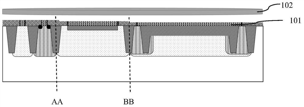
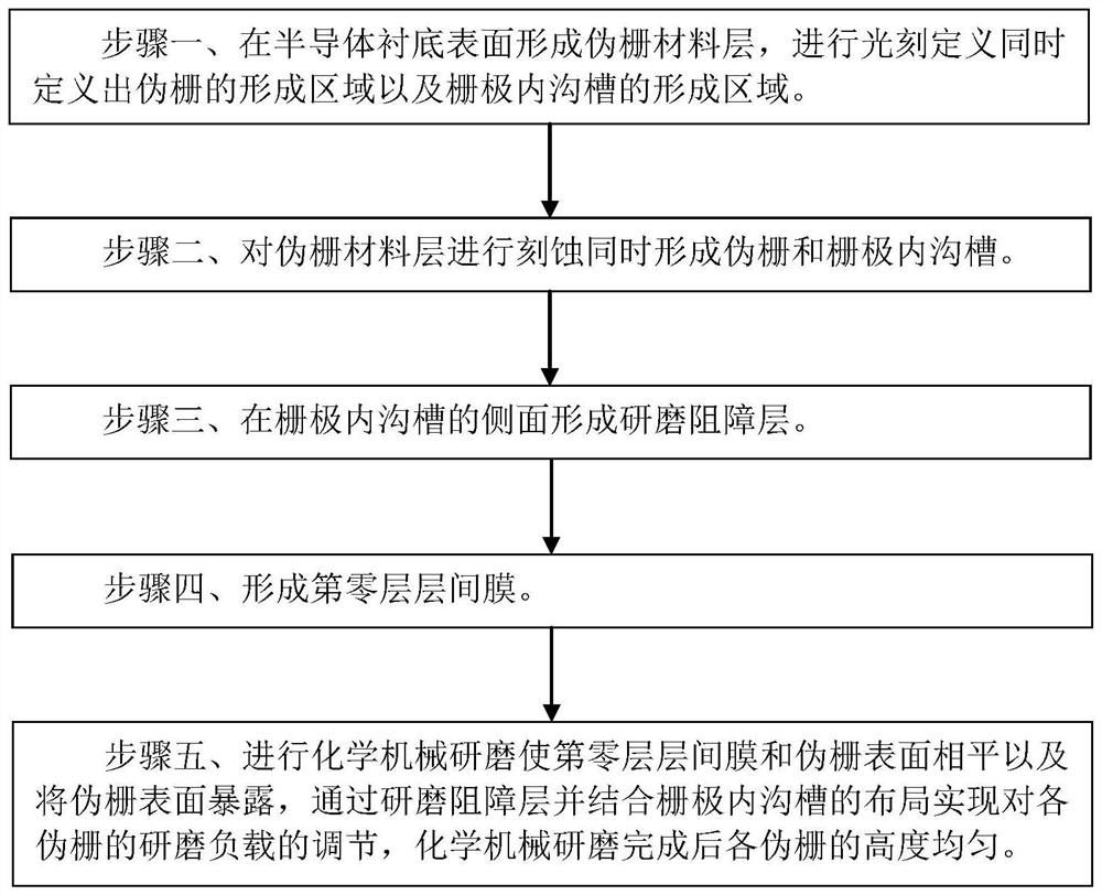
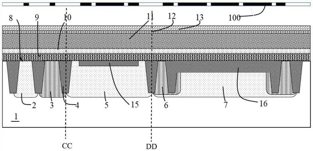
[0042] Such as figure 2 As shown, it is a flow chart of the dummy gate 9 planarization method in the gate-last process of the embodiment of the present invention; Figure 3A to Figure 3F Shown is a schematic diagram of the device structure in each step of the dummy gate 9 planarization method in the gate-last process of the embodiment of the present invention. The method for planarizing the dummy gate 9 in the gate-last process of the embodiment of the present invention includes the following steps:
[0043] Step 1, such as Figure 3A As shown, a dummy gate 9 material layer is formed on the surface of the semiconductor substrate 1, and a mask plate 100 is used for photolithography definition to define the formation area of the dummy gate 9 and the formation area of the trench (slot) 14 in the gate. The dummy gate 9 The length is the dimension along the length direction of the channel, the length of the dummy gate 9 includes a plurality of lengths, and the trench 14 in t...
PUM
 Abstract
Description
Claims
Application Information
 - R&D
- Intellectual Property
- Life Sciences
- Materials
- Tech Scout
- Unparalleled Data Quality
- Higher Quality Content
- 60% Fewer Hallucinations
Browse by: Latest US Patents, China's latest patents, Technical Efficacy Thesaurus, Application Domain, Technology Topic, Popular Technical Reports.
© 2025 PatSnap. All rights reserved.Legal|Privacy policy|Modern Slavery Act Transparency Statement|Sitemap|About US| Contact US: help@patsnap.com