Packaging structure and forming method thereof

A packaging structure and flip-chip technology, which is applied in the manufacture of electrical components, electrical solid devices, semiconductor/solid devices, etc., can solve the problems of reduced connection area on the back of the substrate, limited circuit design of the substrate, and blockage of air holes by plastic packaging materials, etc.

Active Publication Date: 2021-09-14
CHANGXIN MEMORY TECH INC
View PDF12 Cites 2 Cited by
  • Summary
  • Abstract
  • Description
  • Claims
  • Application Information

AI Technical Summary

Problems solved by technology

In order to have a better exhaust effect, multiple air holes are usually formed on the substrate, but since most of the area on the substrate is used to connect with the chip, the area where the air holes can be formed is small and a large number of air holes are formed , so that the size of each air hole is smaller. Although the number of air holes increases, the exhaust position can be increased, but due to the small air hole size, it will be eas

Method used


Image

  • Packaging structure and forming method thereof
  • Packaging structure and forming method thereof
  • Packaging structure and forming method thereof

Examples


Embodiment Construction

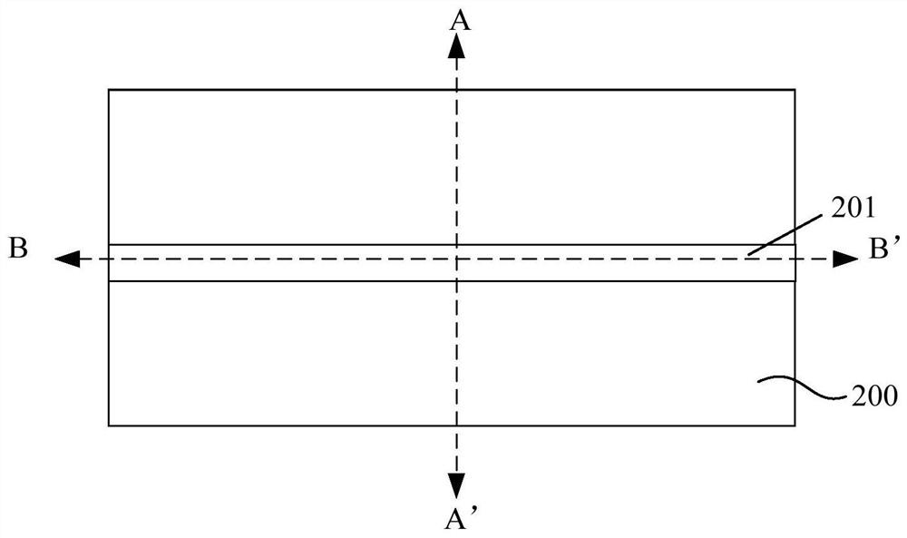
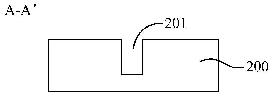
[0033] Please refer to Figure 2A to Figure 2C It is a structural schematic diagram of a substrate of a packaging structure according to a specific embodiment of the present invention, wherein Figure 2A is a schematic top view of the substrate, Figure 2B for the substrate along Figure 2A The cross-sectional schematic diagram of A-A' direction in the middle, Figure 2C for the substrate along Figure 2A The cross-sectional schematic diagram of B-B' direction in the middle.

[0034] The substrate 200, the substrate 200 has opposite first surface and second surface, the first surface is used to fix the chip, and the second surface is used to form solder balls connected with other circuit boards.

[0035] The substrate 200 is a circuit board, and the surface and / or inside of the substrate 200 are formed with electrical connection structures such as interconnection circuits and pads (not shown in the figure), which are used to form an electrical connection with the chip and ...


PUM

PropertyMeasurementUnit
Widthaaaaaaaaaa
Depthaaaaaaaaaa

Abstract

The invention relates to a packaging structure and a forming method thereof. The packaging structure comprises: a substrate, wherein the substrate is provided with a first surface and a second surface which are opposite, the first surface of the substrate is internally provided with at least one long-strip-shaped groove, the two ends of the groove extend to the edge of the substrate and are open ports, and the depth of the groove is smaller than the thickness of the substrate; a chip fixed on the first surface of the substrate in an inverted manner through welding salient points and electrically connected with the substrate through the welding salient points, wherein at least part of the groove is located in the projection of the chip on the substrate; a bottom filling layer, wherein the gap between the chip and the first surface of the substrate is filled with the bottom filling layer; and a plastic packaging layer covering the bottom filling layer and wrapping the chip. According to the packaging structure, internal gas can be effectively exhausted in the injection molding process, and the connecting area of the back face of the substrate is not affected.

Description

technical field [0001] The invention relates to the field of chip packaging, in particular to a packaging structure and a forming method thereof. Background technique [0002] After the chip is packaged, it needs to be packaged by injection molding to protect the chip. [0003] For a chip packaged by a flip chip process (Flip chip), the chip and the substrate are connected to the circuit on the substrate through solder balls. During the plastic encapsulation process, it is necessary to wrap the entire chip with a plastic encapsulant to fill the gap between the chip and the substrate. Since the chip and the substrate are directly connected by solder balls or other solder bumps, the gap is small, and the distance between the connection points is also small. Therefore, the air is not easy to discharge when the plastic encapsulant is filled, and it is easy to be between the chip and the substrate. Bubbles are generated in the plastic encapsulant, which affects the stability of...

Claims


Application Information

Patent Timeline
IPC IPC(8): H01L21/56H01L21/31
CPCH01L21/563H01L23/3128H01L21/31H01L23/13H01L23/49816H01L2224/16227H01L2224/05572H01L2224/0401H01L2224/131H01L2924/15311H01L24/13H01L24/16H01L2924/15159H01L2924/15162H01L2924/014H01L2924/00014H01L24/32H01L24/73H01L24/92H01L2224/32113H01L2224/73204H01L2224/92125H01L2924/15151
Inventor 张志伟
Owner CHANGXIN MEMORY TECH INC
Why Eureka
Try Eureka