Solar cell, back contact structure thereof, cell assembly and photovoltaic system

A technology of solar cells and back contact, applied in the field of solar cells, can solve problems such as belt transmission scratches

Pending Publication Date: 2021-09-14
ZHEJIANG AIKO SOLAR ENERGY TECH CO LTD +3
View PDF0 Cites 4 Cited by
  • Summary
  • Abstract
  • Description
  • Claims
  • Application Information

AI Technical Summary

Problems solved by technology

[0005] The purpose of the embodiments of the present invention is to provide a back contact structure of solar cell

Method used


Image

  • Solar cell, back contact structure thereof, cell assembly and photovoltaic system
  • Solar cell, back contact structure thereof, cell assembly and photovoltaic system
  • Solar cell, back contact structure thereof, cell assembly and photovoltaic system

Examples


Embodiment 1

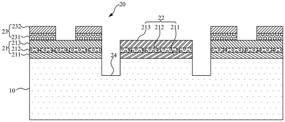
[0057] An embodiment of the present invention provides a back contact structure of a solar cell. For ease of description, only the parts related to the embodiment of the present invention are shown. Refer to figure 1 As shown, the back contact structure 20 of the solar cell provided by the embodiment of the present invention includes:

[0058] A first doped region 21 with a polarity opposite to that of the silicon substrate 10 and a second doped region 22 with the same polarity as that of the silicon substrate 10 are arranged at intervals on the back of the silicon substrate 10, and the first doped region 21 is provided with There are protected areas 23;

[0059] Both the first doped region 21 and the second doped region 22 include a first doped layer 211, a passivation layer 212, and a second doped layer 213;

[0060] The protection region 23 includes an insulating layer 231 and a third doped layer 232 having the same polarity as the second doped region 22;

[0061] An isol...

Embodiment 2

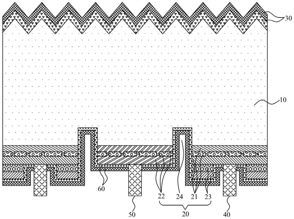
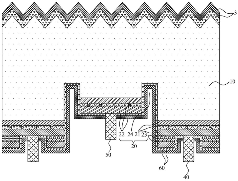
[0089] The second embodiment of the present invention provides a solar cell. For the convenience of description, only the parts related to the embodiment of the present invention are shown. Refer to figure 2 and image 3 As shown, the solar cell provided by the embodiment of the present invention includes:

[0090] silicon substrate 10;

[0091] The back contact structure 20 described in the foregoing embodiments disposed on the back of the silicon substrate 10;

[0092] a first dielectric layer 30 disposed on the front side of the silicon substrate 10;

[0093] a first conductive layer 40 disposed on the first doped region 21 in the back contact structure 20 and a second conductive layer 50 disposed on the second doped region 22 in the back contact structure 20; and

[0094] The second dielectric layer 60 is disposed on the back contact structure 20 and disposed between the first conductive layer 40 and the second conductive layer 50 .

[0095] Wherein, in one embodiment...

Embodiment 3

[0109] The third embodiment of the present invention also provides a battery assembly, which includes the solar cell described in the second embodiment above.


PUM

PropertyMeasurementUnit
Thicknessaaaaaaaaaa
Thicknessaaaaaaaaaa
Thicknessaaaaaaaaaa

Abstract

The invention is applicable to the technical field of solar cells, and provides a solar cell and a back contact structure thereof, a cell assembly and a photovoltaic system, the back contact structure comprises first doped regions which are arranged on the back of a silicon substrate at intervals and have polarities opposite to the polarity of the silicon substrate, and second doped regions which have the same polarities as the polarity of the silicon substrate. Protection regions are arranged on the first doped regions; each of the first doped region and the second doped region comprises a first doped layer, a passivation layer and a second doped layer; each protection region comprises an insulating layer and a third doped layer with the same polarity as the second doped region; isolation regions are arranged between the first doped regions and the second doped regions; the protection regions are provided with openings, so that a first conductive layer is connected with the first doped region; and the heights of the first doped regions and the second doped regions are both higher than the heights of the isolation regions. According to the back contact structure provided by the invention, the problem of scratches caused by belt transmission in the existing battery preparation process is solved.

Description

technical field [0001] The invention belongs to the technical field of solar cells, and in particular relates to a solar cell and its back contact structure, a cell component and a photovoltaic system. Background technique [0002] Solar cell power generation is a sustainable source of clean energy. It uses the photovoltaic effect of semiconductor p-n junctions to convert sunlight into electrical energy, and the conversion efficiency is an important indicator of solar cell performance. IBC (Interdigitated back contact) battery, that is, the interdigitated back contact battery, its positive / negative electrodes are designed on the back of the battery, so that the front surface completely avoids the shielding of the metal grid line, and eliminates the occlusion caused by the metal grid line. Optical loss, and the electrode width can be designed wider than the existing ones, which reduces the series resistance loss, thereby greatly improving the conversion efficiency. In additi...

Claims


Application Information

Patent Timeline
IPC IPC(8): H01L31/0224H01L31/0216H01L31/068
CPCH01L31/022441H01L31/022458H01L31/02167H01L31/02168H01L31/0682Y02E10/547
Inventor 陈刚许文理邱开富王永谦杨新强
Owner ZHEJIANG AIKO SOLAR ENERGY TECH CO LTD
Why Eureka
Try Eureka