Chip and cutting method thereof

A cutting method and chip technology, applied in electrical components, circuits, semiconductor devices, etc., can solve problems such as poor chip cutting

Active Publication Date: 2021-09-14
XIANGNENG HUALEI OPTOELECTRONICS
View PDF5 Cites 0 Cited by
  • Summary
  • Abstract
  • Description
  • Claims
  • Application Information

AI Technical Summary

Problems solved by technology

[0004] The object of the present invention is to provide a chip and it

Method used


Image

  • Chip and cutting method thereof
  • Chip and cutting method thereof
  • Chip and cutting method thereof

Examples


Embodiment 1

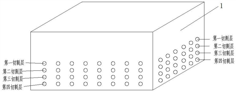
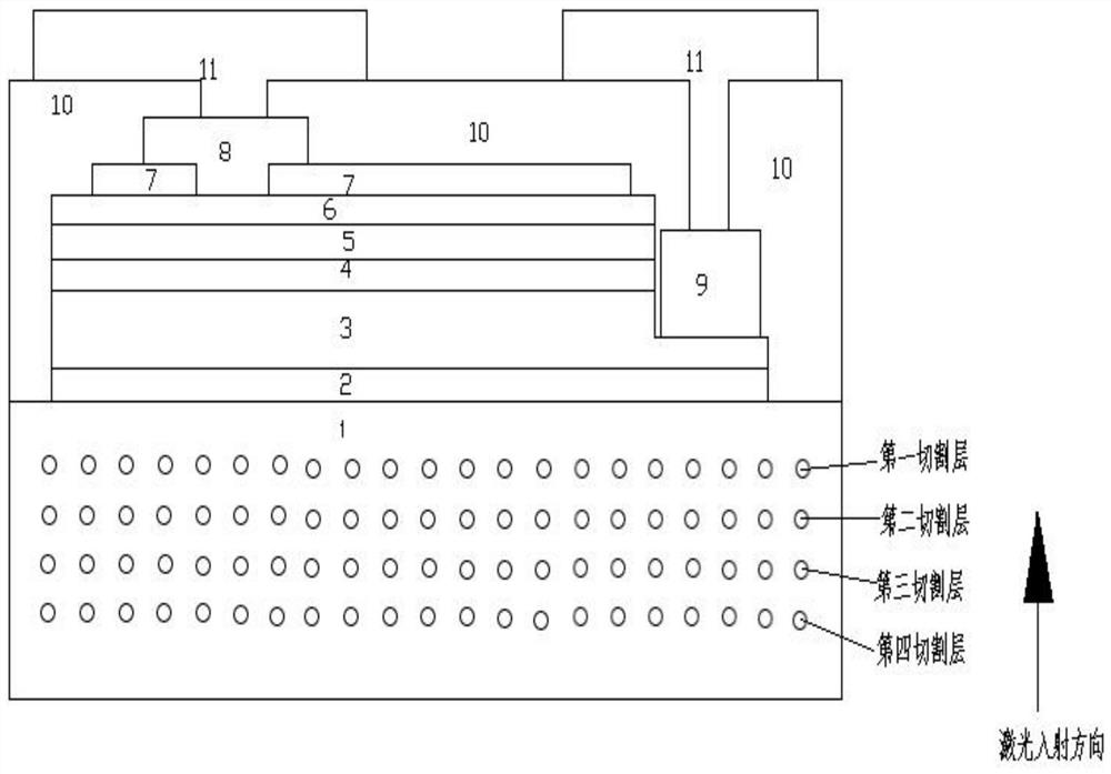
[0029] see Figure 1 to Figure 2 , a chip cutting method, the present embodiment is applied to the cutting of UVC (short-wave ultraviolet) LED chips.

[0030] A chip cutting method, comprising the following steps:

[0031] Step 1. Chip preparation: several chips are prepared on the substrate 1 .

[0032] Step 1.1, grow AlN layer 2, N-type AlGaN layer 3, MQW layer 4, P-type AlGaN layer 5, and P-type GaN layer 6 sequentially on the sapphire substrate 1 through conventional processes to prepare UVC (short-wave ultraviolet) LED epitaxial wafers ;

[0033] Step 1.2, preparing an N electrode layer 9 on the N-type AlGaN layer 3 through an etching process and an electrode contact process on the LED epitaxial wafer;

[0034] Step 1.3: Prepare a current spreading layer 7 with a thickness of 1100A by sputtering or vapor deposition, and carry out alloy treatment on the current spreading layer 7 by means of RTA alloy. process to prepare the pattern of the current spreading layer 7; and...

Embodiment 2

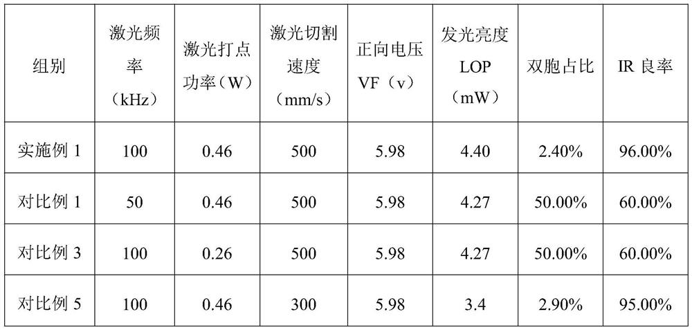
[0052] The difference between this embodiment and embodiment 1 is that in step 2.1, the laser frequency used for the first laser cutting is 90 kHz.

Embodiment 3

[0054] The difference between this embodiment and Embodiment 1 is that in step 2.1, the laser frequency used for the first laser cutting is 110 kHz.


PUM

PropertyMeasurementUnit
Thicknessaaaaaaaaaa
Wavelengthaaaaaaaaaa
Thicknessaaaaaaaaaa

Abstract

The invention provides a chip cutting method, which comprises the steps of preparing chips and cutting the chips, when the chips are cut, substrates of a plurality of chips are cut by adopting a laser stealth cutting process, the laser stealth cutting process comprises at least two times of laser cutting of which the cutting depths are sequentially reduced, wherein the first laser cutting adopts a high-frequency, high-power and high-speed cutting mode; and in the laser dot matrix formed by multiple times of laser cutting, the offset between the same row of laser points arranged in the cutting depth direction is smaller than 10 microns. The invention also provides the chip prepared by adopting the chip cutting method. According to the invention, extending lines generated during laser cutting can be more effectively controlled, so that the side wall of the chip is coarsened, and light can be conveniently taken out; and the stress generated by the first laser cutting can be further released through the subsequent laser cutting, cracks of the side wall of the substrate are further controlled, it is ensured that electric leakage of the chip cannot be caused in the cutting process, and the IR yield of the chip is improved.

Description

technical field [0001] The invention relates to the technical field of chip manufacturing, in particular to a chip and a cutting method thereof. Background technique [0002] With the increase of people's awareness of health concerns, people's demand for sterilization and antivirus products has exploded. UVC (short-wave ultraviolet) LED chips are made of the third-generation semiconductor material GaN, which has a long service life in terms of performance. It is long, safe and environmentally friendly, and can be used for sterilization and disinfection. However, when cutting UVC chips, it is easy to cause poor chip cutting due to immature production technology, and it is easy to produce twin phenomena, resulting in low chip cutting yield, which restricts the development of UVC chips. widely used. [0003] To sum up, there is an urgent need for a chip and its cutting method to solve the problems in the prior art. Contents of the invention [0004] The object of the presen...

Claims


Application Information

Patent Timeline
IPC IPC(8): H01L33/00H01L33/06H01L33/14
CPCH01L33/0075H01L33/007H01L33/06H01L33/14
Inventor 周智斌
Owner XIANGNENG HUALEI OPTOELECTRONICS
Why Eureka
Try Eureka