Single-chip DAF adhesive tape crystal bonding method
A single-chip and adhesive tape technology, which is applied in the direction of electrical components, semiconductor/solid-state device manufacturing, circuits, etc., can solve the problems of uneven adhesive layer and small application range, and achieve the effect of preventing glue overturning
- Summary
- Abstract
- Description
- Claims
- Application Information
AI Technical Summary
Problems solved by technology
Method used
Image

Examples
Embodiment 1
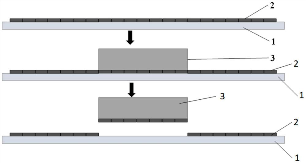
[0032] A kind of single-chip DAF adhesive tape bonding crystal method, comprises the steps: as figure 2 as shown,
[0033] Step 1): Attach the UV photosensitive DAF tape 1 to the bandage ring, cut the DAF tape adhesive layer 2 on the wafer dicing machine into 0.05mm×0.05 mm Small squares of mm size.
[0034] Step 2): Use the pick-up and place device to pick up the front side of a single chip 3, and stick the back side down on the cut DAF tape, and heat and press at a temperature of 60°C and a pressure of 0.1Mpa for 10 seconds. At this time, the bonding of the DAF tape Enhanced layer to chip adhesion.
[0035] Step 3): UV light is irradiated from the back of the tape where the chip is attached, and the intensity of UV light irradiation is > 120mW / cm 2 , so that the adhesive force between the DAF tape adhesive layer and the tape substrate is reduced, and then the chip is removed according to the conventional coring method for subsequent die-bonding operations. At this time, ...
Embodiment 2
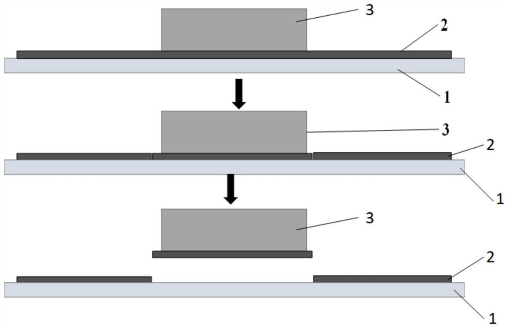
[0037] A kind of single-chip DAF adhesive tape bonding crystal method, such as image 3 shown, including the following steps:
[0038] Step 1): Attach the UV photosensitive DAF tape 1 to the bandage ring, use the suction and placement device to absorb the front of a single chip, attach the back to the DAF tape, and heat it at a temperature of 90°C and a pressure of 0.1Mpa The pressure is applied for 3 seconds, and at this time, the adhesive force between the adhesive layer 2 of the DAF tape and the chip 3 is enhanced.
[0039] Step 2): Cut the DAF adhesive layer on a wafer dicing machine to a size 10 μm larger than the chip size.
[0040] Step 3): UV light is irradiated from the back of the tape where the chip is attached, and the intensity of UV light irradiation is > 120mW / cm 2 , so that the adhesive force between the DAF tape adhesive layer and the tape substrate is reduced, and then the chip is removed according to the conventional coring method for subsequent die-bondin...
Embodiment 3
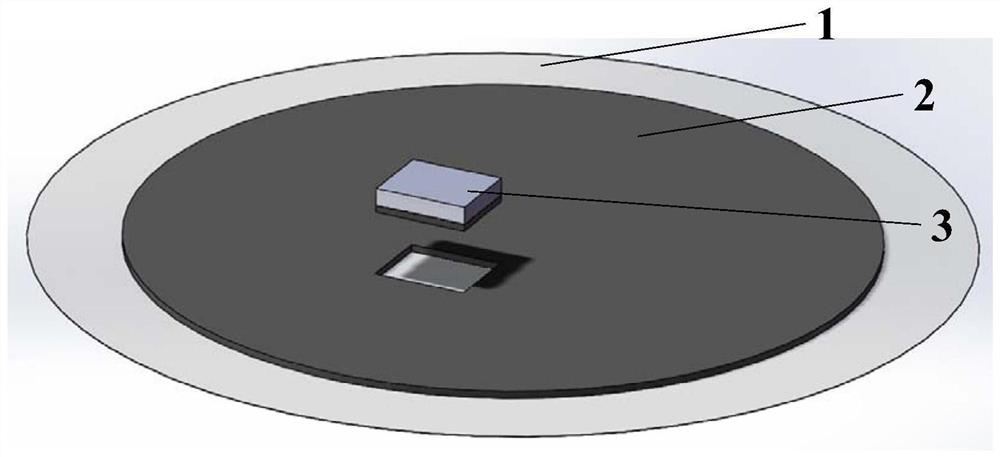
[0042] A kind of single-chip DAF adhesive tape bonding crystal method, such as figure 1 shown, including the following steps:
[0043] Step 1): Attach the UV photosensitive DAF tape 1 to the bandage ring, cut the DAF tape adhesive layer 2 on the wafer dicing machine into 0.05mm×0.05 mm Small squares of mm size.
[0044] Step 2): Use the pick-up and place device to pick up the front side of the single chip 3, stick the back side down on the cut DAF tape, and heat and press at a temperature of 70°C and a pressure of 0.1Mpa for 8 seconds. At this time, the bonding of the DAF tape Enhanced layer to chip adhesion.
[0045] Step 3): UV light is irradiated from the back of the tape where the chip is attached, and the intensity of UV light irradiation is > 120mW / cm 2 , so that the adhesive force between the DAF tape adhesive layer and the tape substrate is reduced, and then the chip is removed according to the conventional coring method for subsequent die-bonding operations. At thi...
PUM
| Property | Measurement | Unit |
|---|---|---|
| Strength | aaaaa | aaaaa |
Abstract
Description
Claims
Application Information
 - R&D
- Intellectual Property
- Life Sciences
- Materials
- Tech Scout
- Unparalleled Data Quality
- Higher Quality Content
- 60% Fewer Hallucinations
Browse by: Latest US Patents, China's latest patents, Technical Efficacy Thesaurus, Application Domain, Technology Topic, Popular Technical Reports.
© 2025 PatSnap. All rights reserved.Legal|Privacy policy|Modern Slavery Act Transparency Statement|Sitemap|About US| Contact US: help@patsnap.com