Manufacturing method of metal thin film and manufacturing method of semiconductor device

A technology of metal thin film and manufacturing method, which is applied in semiconductor/solid-state device manufacturing, electrical components, circuits, etc., can solve the problems of metal thin film etching residue, metal thin film copper precipitation, etc., and achieve the effect of avoiding etching residue and shortening the time

Pending Publication Date: 2021-09-24
SEMICON MFG ELECTRONICS (SHAOXING) CORP
View PDF6 Cites 0 Cited by
  • Summary
  • Abstract
  • Description
  • Claims
  • Application Information

AI Technical Summary

Problems solved by technology

[0004] The purpose of the present invention is to provide a method for manufacturing a metal thin film and a method for manufacturing a semiconductor device, which can avoid the problem of copper precipitation in the metal thin film, thereby avoiding the occurrence of etching residues when the metal thin film is etched.

Method used


Image

  • Manufacturing method of metal thin film and manufacturing method of semiconductor device
  • Manufacturing method of metal thin film and manufacturing method of semiconductor device

Examples


Embodiment Construction

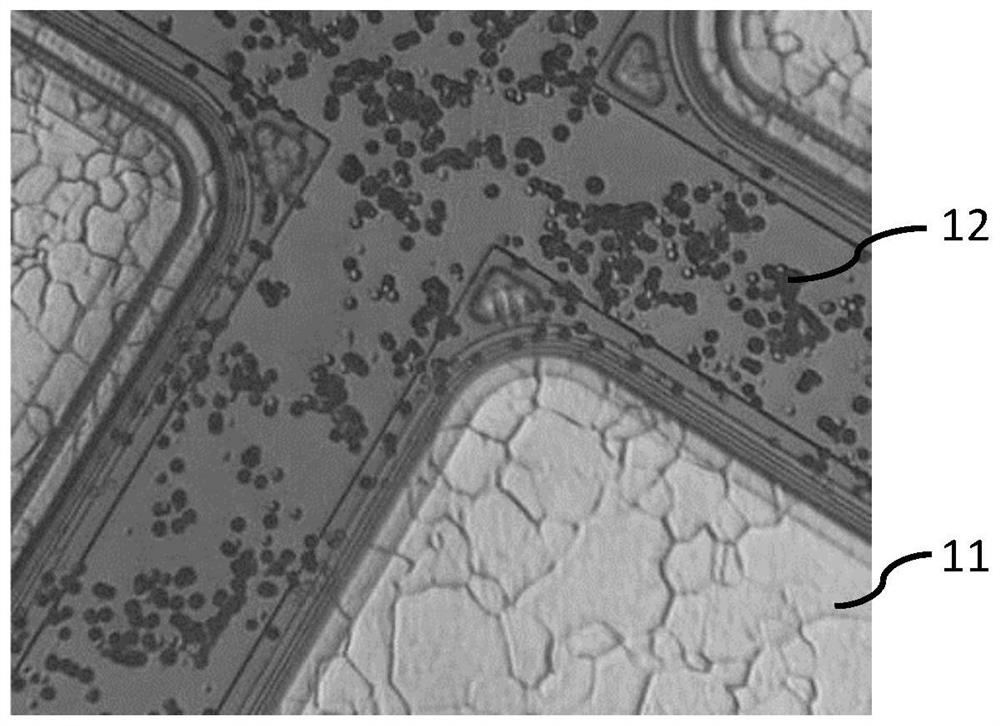
[0035] In order to make the purpose, advantages and features of the present invention clearer, the method for manufacturing the metal thin film and the method for manufacturing the semiconductor device proposed by the present invention will be further described in detail below with reference to the accompanying drawings. It should be noted that all the drawings are in a very simplified form and use imprecise scales, and are only used to facilitate and clearly assist the purpose of illustrating the embodiments of the present invention.

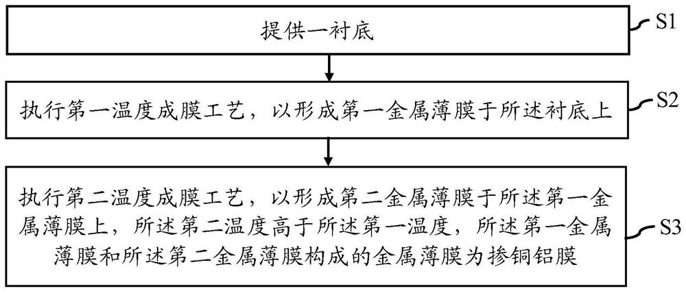
[0036] An embodiment of the present invention provides a method for manufacturing a metal thin film, see figure 2 , figure 2 It is a flowchart of a method for manufacturing a metal thin film according to an embodiment of the present invention, and the method for manufacturing a metal thin film includes:

[0037] Step S1, providing a substrate;

[0038] Step S2, performing a film forming process at a first temperature to form a first metal t...


PUM


Abstract

The invention provides a manufacturing method of a metal film and a manufacturing method of a semiconductor device. The manufacturing method of the metal film comprises the following steps: providing a substrate; executing a first temperature film forming process to form a first metal film on the substrate; and executing a second temperature film forming process to form a second metal film on the first metal film, wherein the second temperature is higher than the first temperature, and a metal film formed by the first metal film and the second metal film is a copper-doped aluminum film. According to the technical scheme, the problem of copper precipitation of the metal film can be avoided, so that etching residues are avoided when the metal film is etched.

Description

technical field [0001] The invention relates to the field of integrated circuit manufacturing, in particular to a method for manufacturing a metal thin film and a method for manufacturing a semiconductor device. Background technique [0002] At present, copper-doped aluminum films are used in many integrated circuits to make metal conductive layers, and if the metal conductive layer is a pad, the metal thin film used to make the pad requires a very high thickness. The existing method of making metal thin films is to complete the substrate in a film-forming chamber in a high-temperature environment at one time, while copper-doped aluminum accumulates more heat with the accumulation of film thickness at high temperatures, which seriously affects the metal thin film. The size of the crystal lattice causes aluminum and copper to form a solid solution, and copper will precipitate out of the solid solution after the metal film is cooled, resulting in the problem of etching residue...

Claims


Application Information

Patent Timeline
Patent Type & Authority Applications(China)
IPC IPC(8): H01L21/02
CPCH01L21/02697
Inventor 张瑜
Owner SEMICON MFG ELECTRONICS (SHAOXING) CORP
Why Eureka
Try Eureka