Calibration device and method for a semiconductor test system

A technology for testing systems and calibration devices, applied to measuring devices, measuring electrical variables, instruments, etc., can solve the problems of slow system software upgrade iterations, time-consuming, and inconvenient maintenance and upgrades, and achieve fast testing and maintenance Convenience and the effect of reducing human error

Active Publication Date: 2021-11-12
NANJING MACROTEST SEMICON TECH CO LTD
View PDF11 Cites 0 Cited by
  • Summary
  • Abstract
  • Description
  • Claims
  • Application Information

AI Technical Summary

Problems solved by technology

If the structure and functions of the function board are modified and upgraded, the corresponding function modules need to be updated synchronously. The test equipment is a very complex system, including many function modules. Modifying a certain part of the program may affect other function modules. Subsequent System software testing will take a lot of time, resulting in inconvenient maintenance and upgrades and poor compatibility
And it will slow down the iteration speed of system software upgrades

Method used


Image

  • Calibration device and method for a semiconductor test system
  • Calibration device and method for a semiconductor test system
  • Calibration device and method for a semiconductor test system

Examples


example

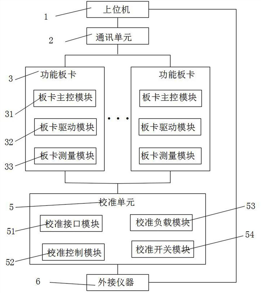
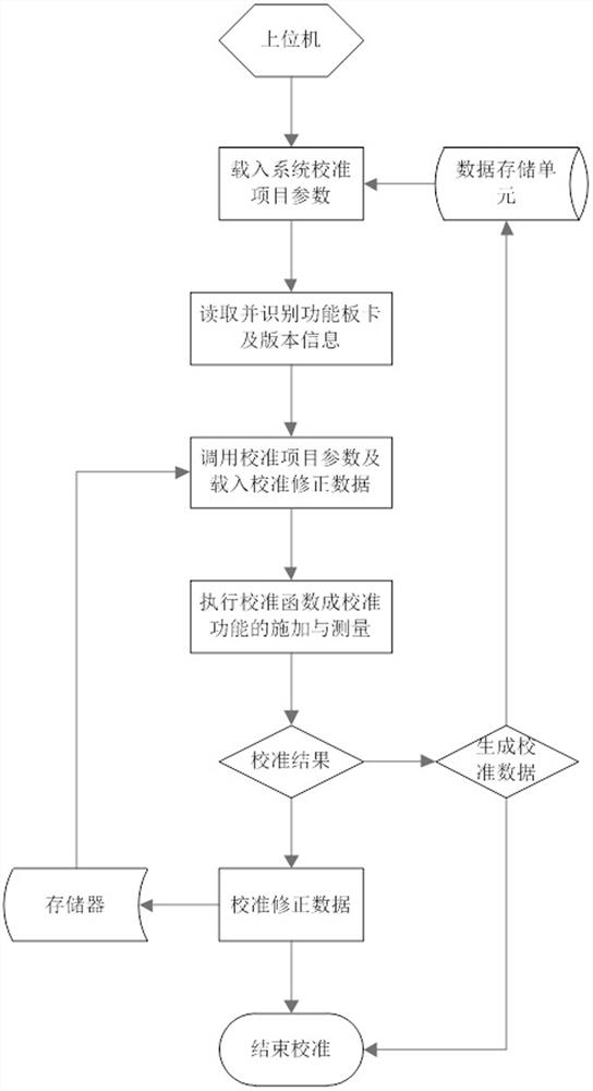
[0042] Such as Figure 1-4 As shown, the user uses the present invention to calibrate the voltage drive function of the functional board 3. First, the system software is started and the system starts to initialize the settings, load the calibration database file to read the preset value of the variable parameter of the calibration item, and then read the function through the function The board and version ID are loaded into the calibration correction data at the same time; next, the software completes the setting of the calibration interface module 51, the calibration switch module 54 and the calibration load module 53 of the calibration unit 5, and then the board main control of the function board 3 The module 31 controls the board driver module 32 to apply voltage, and then controls the external instrument 6 to complete the measurement of the voltage value. At the same time, the host computer 1 analyzes and judges the read measurement data. If the judged calibration result is...


PUM


Abstract

The invention discloses a calibration device and method for a semiconductor test system, which includes a host computer, a communication unit, more than one functional board, a calibration unit, and a data storage unit. The data storage unit stores the parameter specifications designed for system calibration items It is defined as a variable parameter. When the test system software is running, it will automatically identify the calibration item parameter header that needs to be called according to the function board and version ID information, and load it into the system software clock. When the user performs the test system calibration operation, the system The unified programming in the software is a calibration function that conforms to the established rules, and will execute the calibration project parameters to drive the function board and external instruments to complete the calibration work. The invention has the advantages of simple software functions, convenient maintenance, high upgrading efficiency, fast testing, etc., and can reduce human errors in code writing and modification, and improve system stability and compatibility.

Description

technical field [0001] The patent of the present invention relates to the technical field of semiconductor testing, in particular to a calibration device and a calibration method for a semiconductor testing system. Background technique [0002] In the mass production test application of integrated circuits in the semiconductor industry, in order to ensure the authenticity and validity of the test results, it is necessary to regularly calibrate and verify the semiconductor test system to determine whether the functions, accuracy and other indicators of the semiconductor test system meet the design specifications and tests. Requirements, in this process, it is usually necessary to connect each functional board or module inside the test system to the calibration box through cables or interfaces, and then the calibration box is connected to the precision instrument that has passed the verification of a third-party organization to form a complete calibration measurement circuit. ...

Claims


Application Information

Patent Timeline
Patent Type & Authority Patents(China)
IPC IPC(8): G01R35/00
CPCG01R35/005
Inventor 邵凌明毛国梁
Owner NANJING MACROTEST SEMICON TECH CO LTD
Why Eureka
Try Eureka