Method for forming semiconductor structure
A semiconductor and gate structure technology, which is applied in the field of semiconductor structure formation, can solve the problems of poor semiconductor structure performance and reliability, and achieve the effect of increasing the area, increasing the injection angle, and reducing the length.
- Summary
- Abstract
- Description
- Claims
- Application Information
AI Technical Summary
Problems solved by technology
Method used
Image

Examples
Embodiment Construction
[0033] As mentioned in the background art, the performance and reliability of the semiconductor structure formed to overcome the short channel effect of the transistor in the prior art are poor. The following will describe in detail with reference to the accompanying drawings.
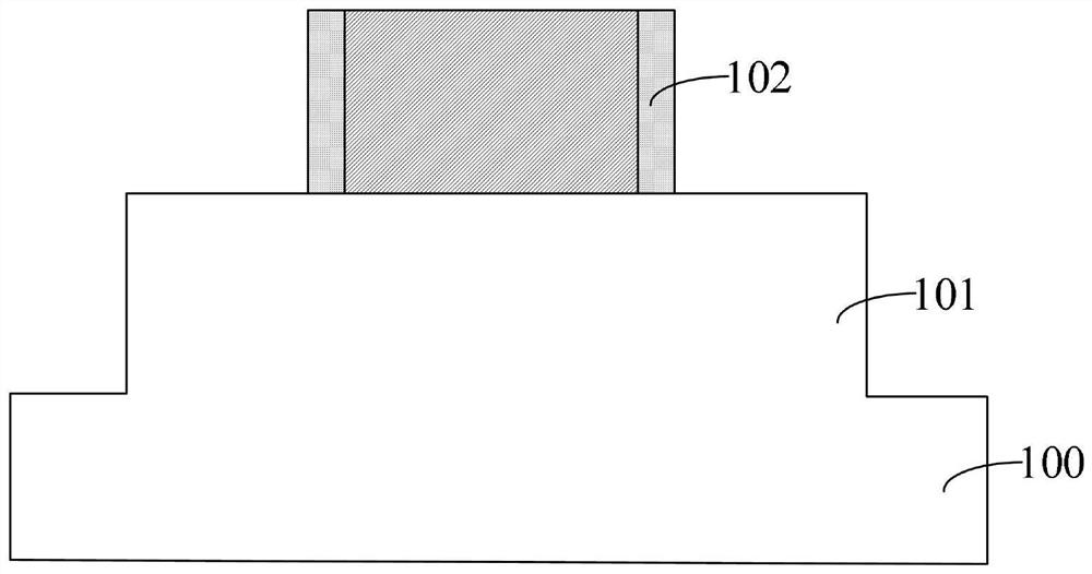
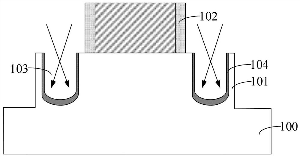
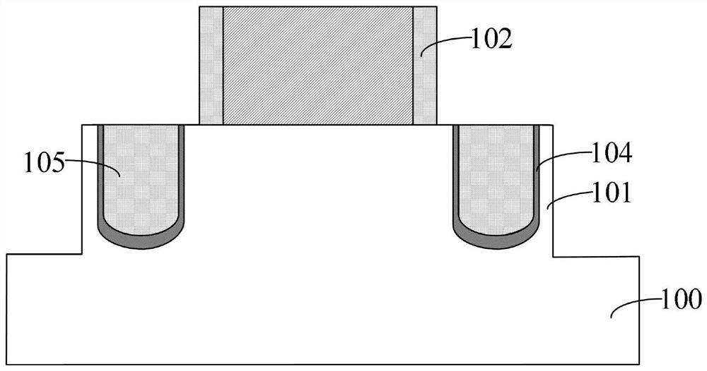
[0034] Figure 1 to Figure 3 It is a structural schematic diagram of each step in the formation process of a semiconductor structure.
[0035] Please refer to figure 1 , providing a substrate 100 with several fins 101 separated from each other on the substrate 100; forming a gate structure 102 on the substrate 100, the gate structure 102 straddling the fins 101, and the The gate structure 102 covers part of the top and sidewall surfaces of the fin 101 .
[0036] Please refer to figure 2 , forming source and drain openings 103 in the fins on both sides of the gate structure 102; performing first ion implantation on the source and drain openings 103, forming in the substrate 100 on the side walls an...
PUM
 Abstract
Description
Claims
Application Information
 - R&D Engineer
- R&D Manager
- IP Professional
- Industry Leading Data Capabilities
- Powerful AI technology
- Patent DNA Extraction
Browse by: Latest US Patents, China's latest patents, Technical Efficacy Thesaurus, Application Domain, Technology Topic.
© 2024 PatSnap. All rights reserved.Legal|Privacy policy|Modern Slavery Act Transparency Statement|Sitemap