Semiconductor device

A semiconductor and conductive technology, applied in semiconductor devices, semiconductor/solid-state device manufacturing, transistors, etc., can solve the problem of reduced damage tolerance and achieve the effect of improving damage tolerance

Pending Publication Date: 2021-09-28
MITSUBISHI ELECTRIC CORP
View PDF1 Cites 0 Cited by
  • Summary
  • Abstract
  • Description
  • Claims
  • Application Information

AI Technical Summary

Problems solved by technology

[0005] However, there is a problem that, in the above-mentioned semiconductor device in which an IGBT and a diode are formed on a single semiconductor substrate, since the IGBT region, terminal region, or gate signal Since the hole injection region such as the gate signal receiving region of the receiving pad is adjacent to the diode region, minority carriers, i.e. holes, flow from the hole injection region to the diode region, reducing the breakdown resistance during recovery operation.

Method used


Image

  • Semiconductor device
  • Semiconductor device
  • Semiconductor device

Examples


Embodiment approach 1

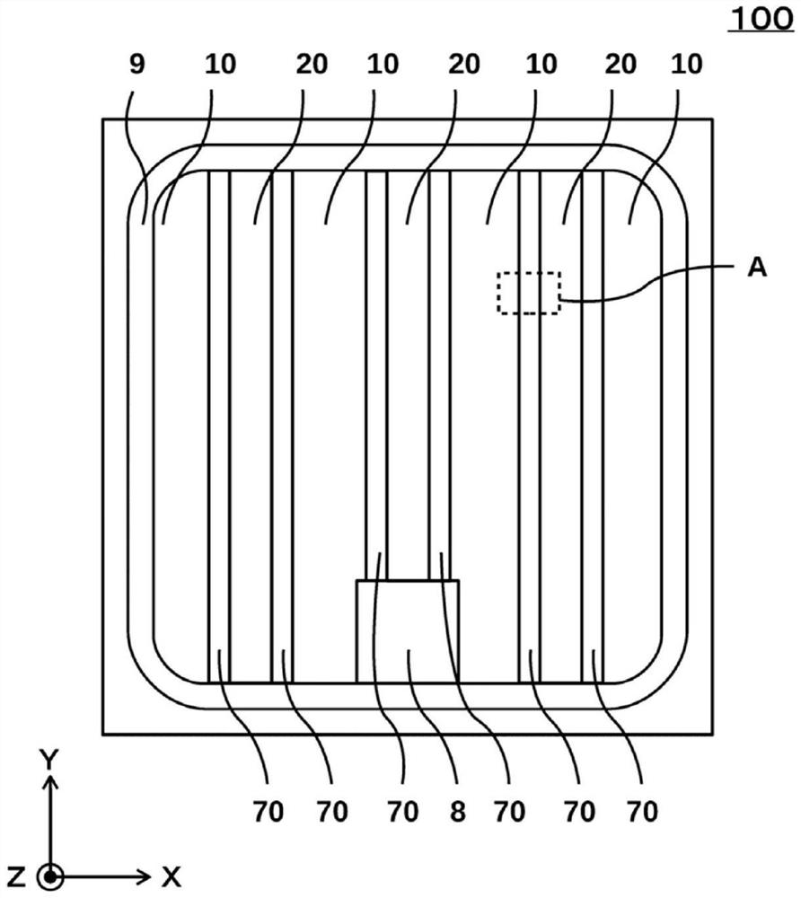
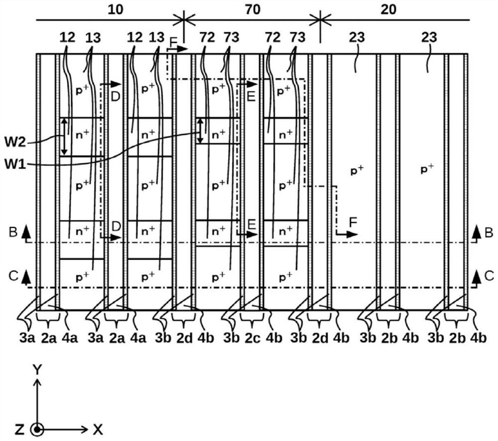
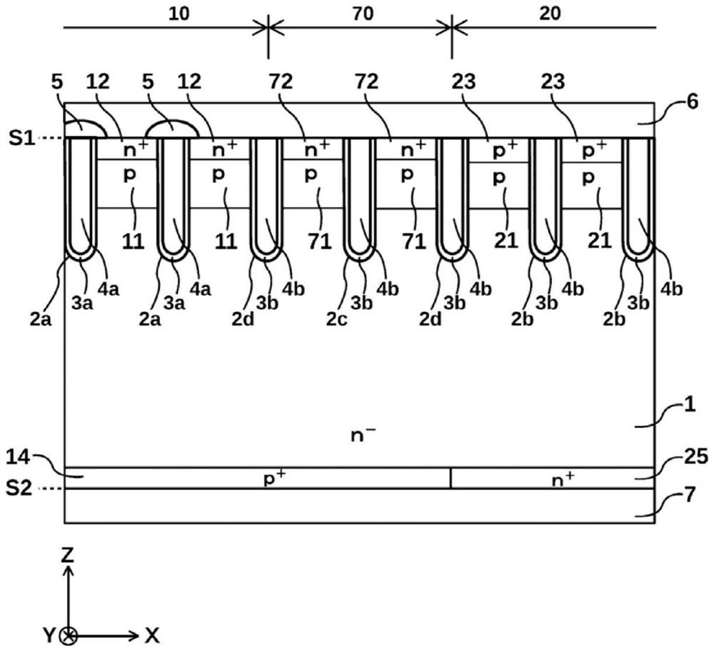
[0048] use Figure 1 to Figure 6 The structure of the semiconductor device according to Embodiment 1 will be described. figure 1 and figure 2 It is a plan view showing the semiconductor device according to the first embodiment. figure 2 will be figure 1 The enlarged plan view of part A described is a plan view showing the structure of the first principal surface side of the semiconductor substrate. exist figure 2 In , the description of the electrodes and the like provided on the upper side of the first main surface of the semiconductor substrate is omitted. Figure 3 to Figure 6 It is a cross-sectional view showing the semiconductor device according to Embodiment 1. image 3 yes figure 2 The sectional view at the line B-B recorded. Figure 4 yes figure 2 The sectional view at line C-C as described. Figure 5 yes figure 2 Sectional view at line D-D as indicated. Figure 6 yes figure 2 Sectional view at line E-E as noted. exist Figure 1 to Figure 6 For conve...

Embodiment approach 2

[0109] use Figure 14 and Figure 15 The structure of the semiconductor device according to Embodiment 2 will be described. Figure 14 and Figure 15 It is a plan view showing the semiconductor device according to the second embodiment. Figure 15 will be Figure 14 The enlarged view of the portion G described is a plan view showing the structure of the first principal surface side of the semiconductor substrate. exist Figure 15 In , the description of the electrodes and the like provided on the upper side of the first main surface of the semiconductor substrate is omitted. exist Figure 14 and Figure 15 For convenience of description, XYZ orthogonal coordinate axes indicating directions are also shown in FIG. In addition, in Embodiment 2, the same constituent elements as those described in Embodiment 1 are given the same reference numerals and descriptions thereof are omitted.

[0110] Such as Figure 14 As shown, the semiconductor device 200 according to Embodime...

Embodiment approach 3

[0113] use Figure 16 to Figure 18 The structure of the semiconductor device according to Embodiment 3 will be described. Figure 16 and Figure 17 It is a plan view showing the semiconductor device according to the third embodiment. Figure 17 will be Figure 16 The enlarged view of part H described is a plan view showing the structure of the first principal surface side of the semiconductor substrate. exist Figure 17 In , the description of the electrodes and the like provided on the upper side of the first main surface of the semiconductor substrate is omitted. Figure 18 yes Figure 17 Sectional view at line J-J as noted. exist Figure 16 to Figure 18 For convenience of description, XYZ orthogonal coordinate axes indicating directions are also shown in FIG. In addition, in Embodiment 3, the same components as those described in Embodiments 1 and 2 are assigned the same reference numerals and description thereof will be omitted.

[0114] Such as Figure 16 As sho...


PUM


Abstract

The invention provides a semiconductor device which can improve the breakdown tolerance during recovery operation. The semiconductor device according to the present application includes: a semiconductor substrate including a first main surface and a second main surface; a hole injection region including a hole injection layer of a second conductivity type and a semiconductor layer of a second conductivity type provided on the second main surface side; a diode region including: an anode layer of a second conductivity type provided on the first main surface side and a cathode of a first conductivity type on the second main surface side, the diode region having no semiconductor layer of a first conductivity type between the second main surface side end portion of the anode layer and the first main surface of the anode layer; a boundary region including: a boundary portion semiconductor layer of a second conductivity type provided on the first main surface side, a carrier injection suppression layer of a first conductivity type provided in a surface layer of the boundary portion semiconductor layer, and the semiconductor layer of a second conductivity type provided to protrude from the hole injection region on the second main surface side, which are arranged between the diode region and the hole injection region.

Description

technical field [0001] The present invention relates to semiconductor devices. Background technique [0002] From the viewpoint of energy saving, inverter devices are widely used in fields such as home appliances, electric vehicles, and railways. Many inverter devices are configured using an insulated gate bipolar transistor (IGBT: Insulated Gate Bipolar Transistor) and a freewheeling diode. The insulated gate bipolar transistor and the diode are connected by wiring such as wires inside the inverter device. [0003] In order to downsize an inverter device, a semiconductor device in which an insulated gate bipolar transistor and a diode are formed on a single semiconductor substrate has been proposed (for example, Patent Document 1). [0004] Patent Document 1: Japanese Patent Laid-Open No. 2008-103590 [0005] However, there is a problem that, in the above-mentioned semiconductor device in which an IGBT and a diode are formed on a single semiconductor substrate, since the...

Claims


Application Information

Patent Timeline
Patent Type & Authority Applications(China)
IPC IPC(8): H01L29/06H01L29/739H01L27/06
CPCH01L27/0629H01L29/7398H01L29/7397H01L29/0615H01L29/8613H01L29/407H01L29/0692H01L29/861H01L27/0727H01L29/0603H01L29/0834H01L29/0696H01L29/1095H01L21/761H01L27/0664H01L29/66348H01L21/765H01L29/66136
Inventor 池田宗谦曾根田真也原田健司
Owner MITSUBISHI ELECTRIC CORP
Why Eureka
Try Eureka