
Lead frame and method for plating lead frame

A lead frame, coating lead technology, applied in electrical components, electrical solid devices, circuits, etc., can solve the problem of harmful effects of solder, achieve good corrosion resistance, good solder wettability, and improve work efficiency.

Inactive Publication Date: 2004-01-14
SAMSUNG AEROSPACE IND
View PDF4 Cites 0 Cited by
  • Summary
  • Abstract
  • Description
  • Claims
  • Application Information

AI Technical Summary

Problems solved by technology

For example, sealing techniques generally require temperatures above 250°C, which will have a detrimental effect on the solder

Method used


Image

  • Lead frame and method for plating lead frame
  • Lead frame and method for plating lead frame
  • Lead frame and method for plating lead frame

Examples


Embodiment Construction

[0023] The invention will be described more fully hereinafter with reference to the accompanying drawings, in which preferred embodiments of the invention are illustrated. However, the invention may be embodied in many different forms and should not be construed as limited to the embodiments set forth herein; rather, the embodiments are provided so that this disclosure will be thorough and complete, and will fully convey to those skilled in the art scope of the invention. Like reference numerals are used throughout to refer to like parts.

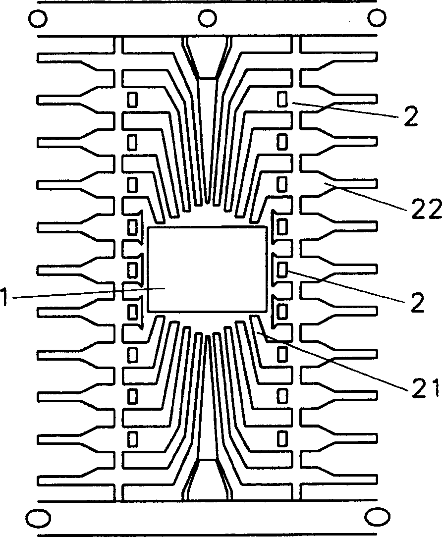
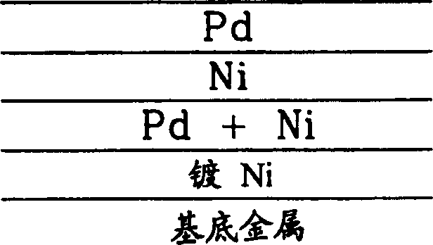
[0024] A preferred embodiment of the lead frame of the present invention will now be described in detail, an example of which is shown in the accompanying drawings. here, Figure 4 is a schematic cross-sectional view of a lead frame coated according to a preferred embodiment of the present invention.

[0025] Such as Figure 4 As shown, the lead frame includes a die pad unit 1 and leads 2 formed on both sides of the die pad unit 1 . Fo...


PUM

PropertyMeasurementUnit
Thicknessaaaaaaaaaa

Abstract

The lead frame includes outer leads plated with tin (Sn) alloy so as to withstand the high temperatures generated during a subsequent semiconductor packaging process. In addition to the outer leads, the lead frame includes a die pad and inner leads composed of a base metal, such as copper (Cu), a copper alloy, or a nickel alloy. The die pad and the inner leads are plated with silver for improved conductivity. In order to withstand relatively high temperatures as well as to resist corrosion and have good solder wettability, the outer leads are preferably plated with a tin antimony alloy, such as a tin-antimony alloy consisting of 90+ / -5 weight percent of tin and 10+ / -5 weight percent antimony. Alternatively, the outer leads can be plated with a tin-antimony-lead alloy, such as a tin-antimony-lead alloy consisting of 10+ / -5 weight percent of tin, 10+ / -5 weight percent of antimony and 80+ / -10 weight percent of lead. A method of plating a lead frame is also provided.

Description

technical field [0001] The present invention relates generally to a lead frame and a method of coating a lead frame, and more particularly to a lead frame and at least partial coating of the lead frame with a tin (Sn) alloy to make it easy to withstand the occurrence of subsequent semiconductor packaging processes. high temperature method. Background technique [0002] During the manufacture of integrated circuit devices (also known as semiconductor chips), packages are formed that seal the integrated circuits. The packages are usually made of a plastic material such as epoxy, although ceramic packages can also be used. To establish the connection of each input / output terminal of the encapsulated chip, a lead frame is also formed and at least partially encapsulated within the package. By wire-bonding each input / output terminal of the semiconductor chip to the lead frame prior to encapsulation, each input / output terminal of the semiconductor chip can be connected to each in...

Claims


Application Information

Patent Timeline
IPC IPC(8): H01L23/495
CPCH01L2924/0002H01L23/49582H01L2924/00
Inventor 金重道白领昊
Owner SAMSUNG AEROSPACE IND
Learn More