a ce 3+ halide electroluminescent device

A halide electroluminescence and electroluminescence technology, which is applied in the fields of electric solid state devices, semiconductor/solid state device manufacturing, electrical components, etc., can solve the problems of poor performance of new non-lead metal halide materials, and achieve high-efficiency electroluminescence applications, Wide application range and high photoluminescence quantum yield

Active Publication Date: 2022-05-20
HUAZHONG UNIV OF SCI & TECH
View PDF15 Cites 0 Cited by
  • Summary
  • Abstract
  • Description
  • Claims
  • Application Information

AI Technical Summary

Problems solved by technology

[0005] The purpose of the present invention is to provide a Ce 3+ Based halide electroluminescent devices aimed at addressing the poor performance of new lead-free metal halide materials for LED applications

Method used


Image

  • a ce  <sup>3+</sup> halide electroluminescent device
  • a ce  <sup>3+</sup> halide electroluminescent device
  • a ce  <sup>3+</sup> halide electroluminescent device

Examples


Embodiment 1

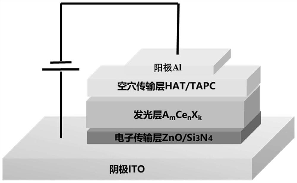
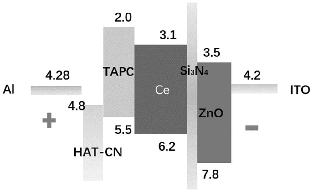
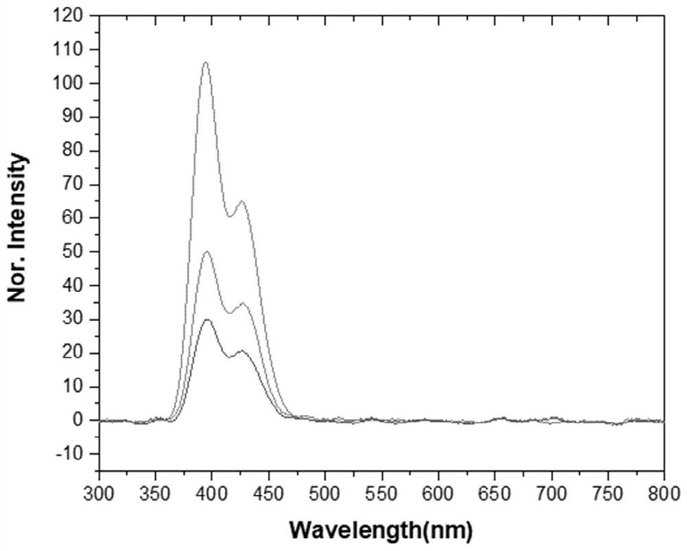
[0037] In this embodiment, the light-emitting layer material is Cs 3 CaBr 6 The violet LED device of the material is taken as an example, and its specific preparation method includes the following steps:

[0038] a) Ultrasonic cleaning of the ITO substrate with detergent, deionized water, acetone and absolute ethanol in sequence for half an hour each time;

[0039] b) Using magnetron sputtering method on ITO, sputtering ZnO with a thickness of about 40nm;

[0040] c) Coating a layer of 10nm Si on ZnO by MOCVD 3 N 4 film;

[0041] d) will be plated Si 3 N 4 The substrate of the film is placed in the evaporation glove box, and the vacuum degree is evacuated to 4*10 -5 Below Pa, the substrate is heated to 200°C, and CeBr is evaporated at a speed of 0.1nm / s by co-evaporation 3 , CsBr was evaporated at a speed of 0.3nm / s, and the total thickness was about 100nm. In the dual-source co-evaporation process, using the spontaneous crystallization process, the CsBr and CeBr 3 T...

Embodiment 2

[0049] In this embodiment, the light-emitting layer material is Cs 3 CaBr 6 The violet LED device of the material is taken as an example, and its specific preparation method includes the following steps:

[0050] a) Clean the base ITO ultrasonically with detergent, deionized water, acetone and absolute ethanol in sequence, half an hour each time;

[0051] b) Using magnetron sputtering method on ITO, sputtering ZnO with a thickness of about 40nm;

[0052] c) A layer of 10nm Al is plated on ZnO by ALD 2 o 3 film;

[0053] d) will be plated Al 2 o 3 The substrate of the film is placed in the evaporation glove box, and the vacuum degree is evacuated to 4*10 -5 Below Pa, the substrate is heated to 200°C, and CeBr is evaporated at a speed of 0.1nm / s by co-evaporation 3 , CsBr was evaporated at a speed of 0.3nm / s, and the total thickness was about 100nm. In the dual-source co-evaporation process, using the spontaneous crystallization process, the CsBr and CeBr 3 The reactio...

Embodiment 3

[0057] In this embodiment, the light-emitting layer material is Cs 3 CaBr 6 The violet LED device of the material is taken as an example, and its specific preparation method includes the following steps:

[0058] a) Clean the base ITO ultrasonically with detergent, deionized water, acetone and absolute ethanol in sequence, half an hour each time;

[0059] b) Using magnetron sputtering method on ITO, sputtering ZnO with a thickness of about 40nm;

[0060] c) Coating a layer of 10nm NiO thin film on ZnO by MOCVD method;

[0061] d) Put the substrate coated with NiO film into the evaporation glove box, and pump the vacuum to 4*10 -5 Below Pa, the substrate is heated to 200°C, and CeBr is evaporated at a speed of 0.115nm / s by co-evaporation 3 , CsBr was evaporated at a speed of 0.16nm / s, and the total thickness was about 100nm. In the dual-source co-evaporation process, using the spontaneous crystallization process, the CsBr and CeBr 3 The reaction produces Cs 3 CaBr 6 . ...


PUM


Abstract

The invention belongs to the field of optoelectronic devices and discloses a Ce 3+ A halide-based electroluminescent device, which comprises a top electrode, a hole injection layer, a hole transport layer, a light emitting layer, a hole blocking layer, an electron transport layer and a bottom electrode from top to bottom, wherein the light emitting layer adopts The material is Ce 3+ Based halide materials, the general structure of which is A m Ce n x k , wherein A is one or more of Na, K, Rb, and Cs, X is one or more of Cl, Br, and I, and the chemical valence state of Ce is +3, m+3n=k; the Ce-like halide materials have high photoluminescence efficiency, excellent thermal stability and short excited state lifetime, and can be used in electroluminescent devices. The hole transport layer and the electron transport layer are used to inject holes and electrons into the light emitting layer, respectively. The electroluminescent device has the characteristics of simple preparation process, lower cost and low toxicity.

Description

technical field [0001] The invention belongs to the field of optoelectronic devices, more specifically, relates to a Ce 3+ based halide electroluminescent devices. Background technique [0002] In recent years, metal halide materials have developed rapidly in the field of display due to their high photoluminescence quantum yield, good charge transport ability and excellent color purity, and have attracted great attention from the scientific and technological circles and business circles. The efficiency of light-emitting diodes (LEDs) based on metal halide materials has exceeded 20%, which is comparable to the efficiency of commercial organic light-emitting diodes. However, the current research on high-efficiency metal halide light-emitting diodes is mainly based on lead-based perovskite materials. Lead is a The content of neurotoxic heavy metal elements should be strictly controlled in practical applications. [0003] Therefore, the development of new low-toxicity non-lead...

Claims


Application Information

Patent Timeline
Patent Type & Authority Patents(China)
IPC IPC(8): H01L51/50H01L51/54H01L51/56
CPCH10K71/12H10K85/30H10K50/115Y02B20/00
Inventor 罗家俊唐江郭庆勋杨龙波王亮段家顺
Owner HUAZHONG UNIV OF SCI & TECH
Why Eureka
Try Eureka