Tri-gate Ga2O3 transverse MOSFET power device and preparation method thereof
A power device and lateral technology, applied in the field of microelectronics, can solve the problems of restricting the development of SiC power devices, low channel mobility, and many defects, and achieve the advantages of improving short-circuit withstand capability, increasing mobility, and reducing saturation current density. Effect
- Summary
- Abstract
- Description
- Claims
- Application Information
AI Technical Summary
Problems solved by technology
Method used
Image
Examples
Embodiment 1
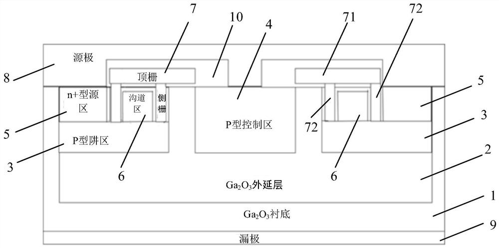
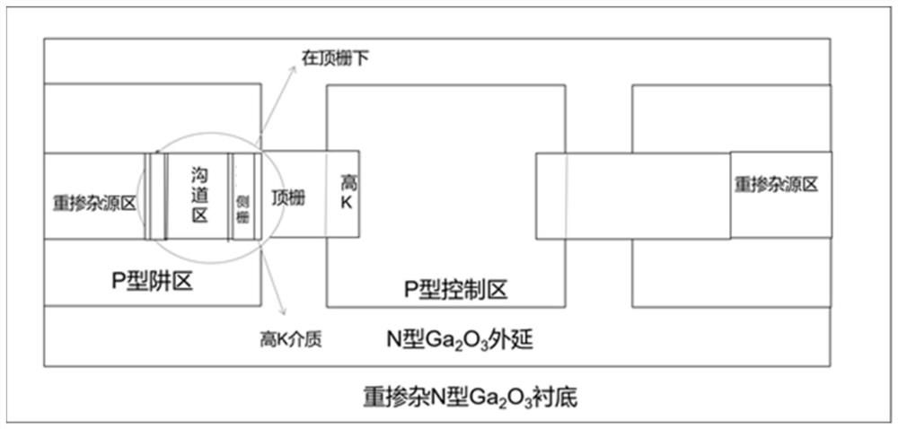
[0046] See figure 1 and figure 2 , figure 1 It is a tri-gate Ga 2 o 3 Schematic cross-sectional view of a lateral MOSFET power device; figure 2 It is a tri-gate Ga 2 o 3 Partial top view of a lateral MOSFET power device. The tri-gate Ga 2 o 3 Lateral MOSFET power devices include Ga 2 o 3 Substrate 1, Ga 2 o 3 Epitaxial layer 2 , two P-type well regions 3 , P-type control region 4 , n+ type source region 5 , channel region 6 , gate 7 , source 8 and drain 9 . In this embodiment, the heavily doped N-type Ga 2 o 3 The material is used as the substrate, and the doping concentration is greater than 1×10 19 cm -3 . Ga 2 o 3 A substrate groove is opened on the substrate 1, Ga 2 o 3 The epitaxial layer 2 is disposed in the substrate groove. In this example, Ga 2 o 3 The height of the epitaxial layer 2 is equal to the depth of the substrate groove, Ga 2 o 3 The epitaxial layer 2 is N-type lightly doped, with a doping concentration of 1×10 14 -1×10 17 cm -3...
Embodiment 2
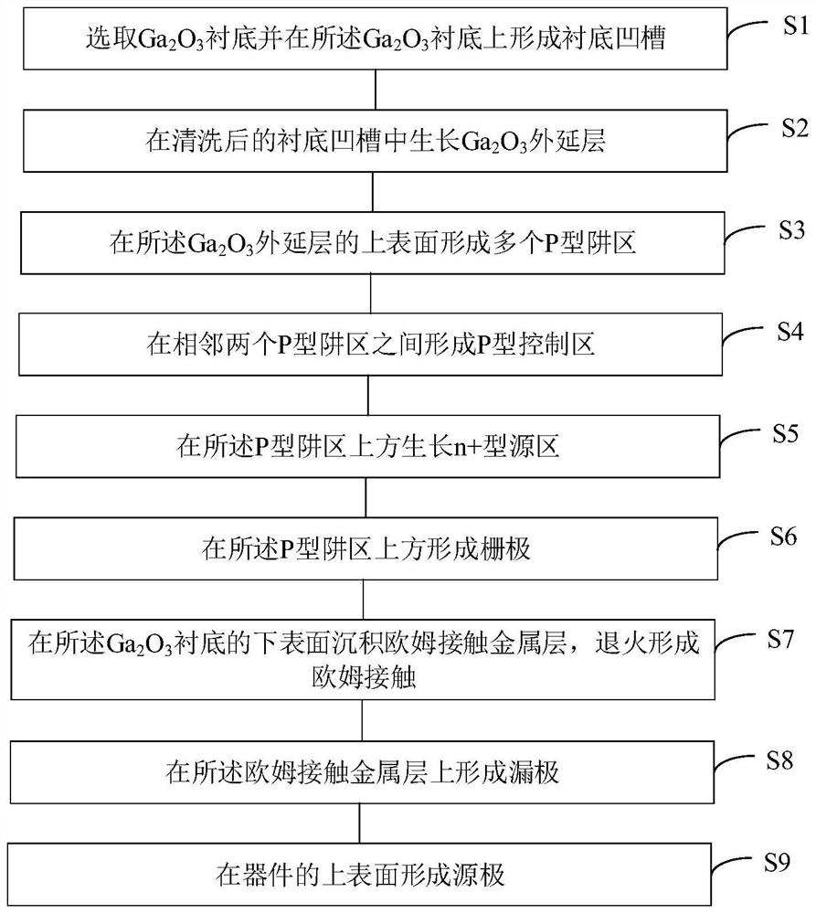
[0055] On the basis of the above embodiments, this embodiment provides a tri-gate Ga 2 o 3 A method for fabricating a lateral MOSFET power device. See image 3 , image 3 It is a tri-gate Ga 2 o 3 Flowchart of the fabrication method for lateral MOSFET power devices. The preparation method includes:
[0056] S1: Choose Ga 2 o 3 substrate and the Ga 2 o 3 A substrate groove is formed on the substrate.
[0057] Specifically, select heavily doped N-type Ga 2 o 3 material as the substrate, using an etching process on the Ga 2 o 3 A substrate groove is formed on the upper surface of the substrate, and then the substrate is cleaned, specifically with acetone and isopropanol solutions for 30-60 seconds, rinsed with deionized water, and finally dried with high-purity nitrogen.
[0058] Preferably, Ga 2 o 3 The doping concentration of the substrate is 1×10 16 -1×10 21 cm -3 , with a thickness of 200-400 μm.
[0059] S2: Growing Ga in the substrate groove after clean...
PUM
| Property | Measurement | Unit |
|---|---|---|
| thickness | aaaaa | aaaaa |
| thickness | aaaaa | aaaaa |
Abstract
Description
Claims
Application Information


