
Double-junction Ga2O3 device and preparation method thereof

A double junction and device technology, applied in the field of microelectronics, can solve the problems of inability to make breakthroughs in double junction semiconductor devices, slow ultraviolet light exploration and detection time, low carrier mobility, etc., to achieve excellent chip performance and improve stability. and electrical properties, the effect of improving mobility

Active Publication Date: 2021-10-26
ZHEJIANG XINKE SEMICON CO LTD
View PDF13 Cites 0 Cited by
  • Summary
  • Abstract
  • Description
  • Claims
  • Application Information

AI Technical Summary

Problems solved by technology

Due to the low carrier mobility and limited withstand voltage of SiC, traditional double-junction SiC devices cannot make breakthroughs in traditional double-junction semiconductor devices; and the detection time of double-junction SiC devices for ultraviolet light exploration Slow and cannot be used in the actual industry

Method used


Image

  • Double-junction Ga2O3 device and preparation method thereof
  • Double-junction Ga2O3 device and preparation method thereof
  • Double-junction Ga2O3 device and preparation method thereof

Examples


Embodiment 1

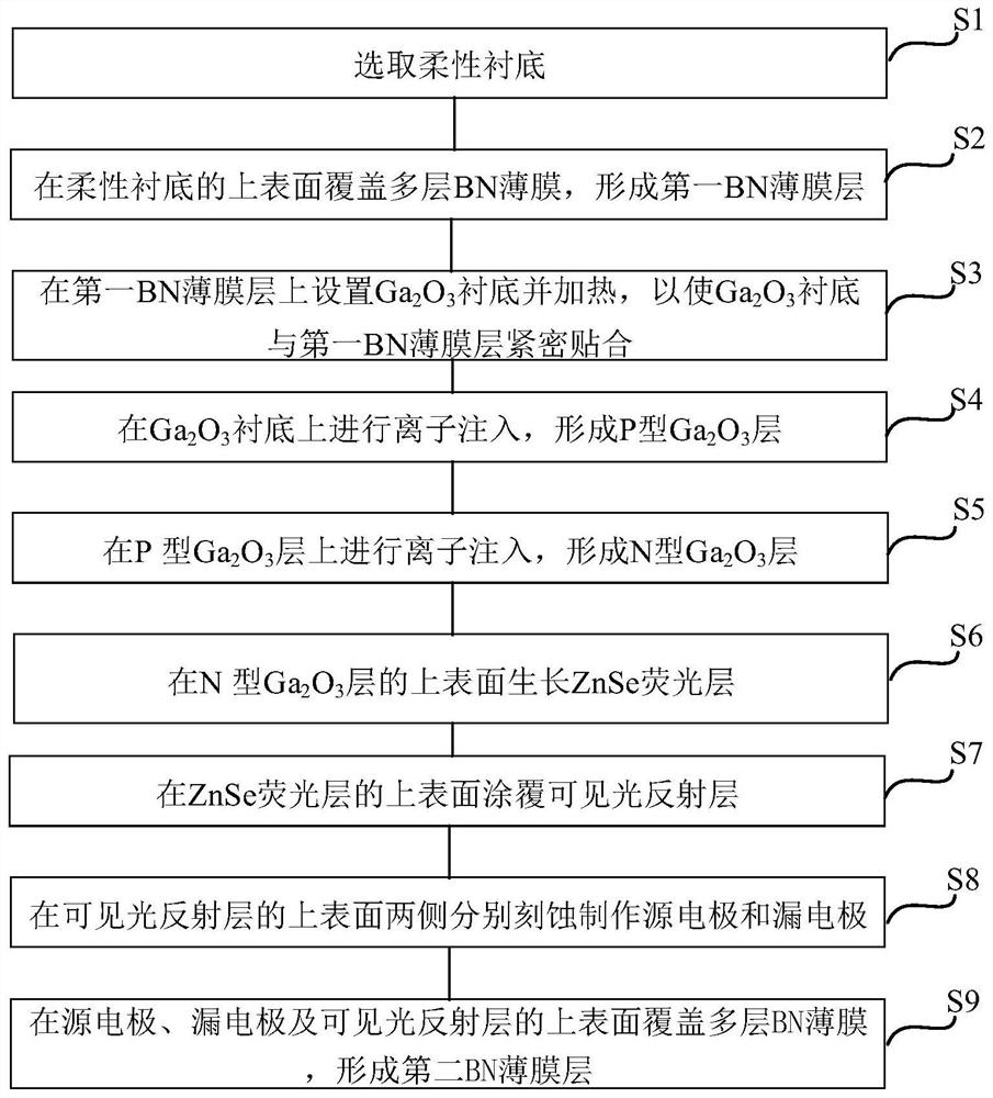
[0040] See figure 1 , figure 1 It is a kind of double-junction Ga 2 o 3 Flowchart of the fabrication method of the device. The double junction Ga 2 o 3 The preparation method of the device includes:

[0041] S1: Select a flexible substrate.

[0042] The flexible substrate is a PET (Polyethyleneterephthalate, polyester resin) flexible substrate with a thickness of 1-2 mm, a length of 2-3 cm, and a width of 2-3 cm. The thickness of the flexible substrate is selected to ensure that when strained, the strain can be precisely applied to the device.

[0043] S2: covering the upper surface of the flexible substrate with multiple layers of BN thin films to form a first BN thin film layer.

[0044] Specifically, a square BN film with 5-10 layers, a total thickness of 5-10 nm, and a size of about 80-120 μm is transferred and placed on the center of the upper surface of the PET flexible substrate using a transfer platform. The 5-10 layers of the BN thin film do not affect the ov...

Embodiment 2

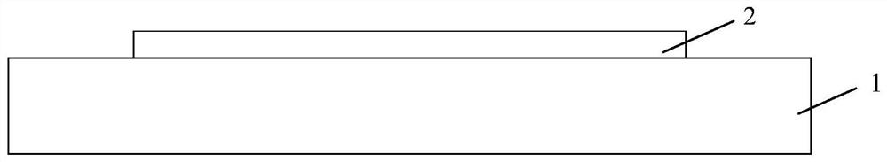
[0059] On the basis of Embodiment 1, this embodiment describes in detail a double-junction Ga 2 o 3 Device fabrication method. See Figure 2a to Figure 2g , Figure 2a to Figure 2g It is a schematic diagram of the preparation process of a double-junction Ga2O3 device provided by the embodiment of the present invention. The preparation method of the present embodiment comprises:

[0060] Step 1: Select a flexible substrate 1, which is a PET flexible substrate with a thickness of 2mm, a length of 3cm, and a width of 3cm.

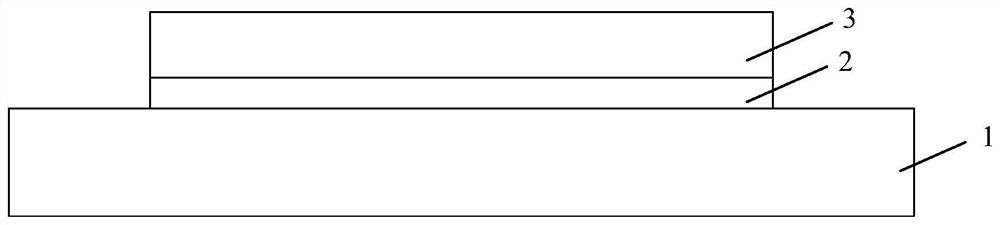
[0061] Step 2: Using a transfer platform, transfer a square BN film with a thickness of 5 layers, a total thickness of 5 nm, and a size of about 100 μm to the center of the above-mentioned PET flexible substrate to form the first BN film layer 2, as Figure 2a shown.

[0062] Step 3: Using the transfer platform to epitaxially grow the 150 thick Ga 2 o 3 The substrate 3 was transferred to the BN thin film and heated at 200°C to make the Ga 2 o 3 The s...

Embodiment 3

[0072] On the basis of the above embodiments, this embodiment provides a double-junction Ga 2 o 3device. like Figure 2g As shown, the double junction Ga 2 o 3 The device includes a flexible substrate 1, a first BN film layer 2, a Ga 2 o 3 Substrate 3, P-type Ga 2 o 3 Layer 4, N-type Ga 2 o 3 Layer 5, ZnSe fluorescent layer 6, visible light reflection layer 7, source electrode 8, drain electrode 9 and second BN thin film layer 10, wherein, flexible substrate 1, first BN thin film layer 2, Ga 2 o 3 Substrate 3, P-type Ga 2 o 3 Layer 4, N-type Ga 2 o 3 Layer 5, ZnSe fluorescent layer 6 and visible light reflective layer 7 are arranged sequentially from bottom to top; source electrode 8 and drain electrode 9 are respectively located on the P-type Ga 2 o 3 Layer 4, N-type Ga 2 o 3 layer 5, ZnSe fluorescent layer 6 and the two sides of the laminated structure formed by the visible light reflective layer 7, and the lower surfaces of the source electrode 8 and the d...


PUM

PropertyMeasurementUnit
thicknessaaaaaaaaaa
thicknessaaaaaaaaaa
thicknessaaaaaaaaaa

Abstract

The invention discloses a double-junction Ga2O3 device and a preparation method thereof. The preparation method comprises the following steps: selecting a flexible substrate; covering the upper surface of the flexible substrate with multiple layers of BN films to form a first BN film layer; arranging a Ga2O3 substrate on the first BN thin film layer and heated, so that the Ga2O3 substrate and the first BN thin film layer are tightly attached; carrying out ion implantation on the Ga2O3 substrate to form a P-type Ga2O3 layer; performing ion implantation on the P-type Ga2O3 layer to form an N-type Ga2O3 layer; growing a ZnSe fluorescent layer on the upper surface of the N-type Ga2O3 layer; coating a visible light reflecting layer on the upper surface of the ZnSe fluorescent layer; respectively etching two sides of the upper surface of the visible light reflecting layer to manufacture a source electrode and a drain electrode; and covering a plurality of layers of BN films on the upper surfaces of the source electrode, the drain electrode and the visible light reflecting layer to form a second BN film layer. The double-junction Ga2O3 device has excellent chip performance, can bear higher temperature and voltage, and can be applied to high-voltage and high-power equipment and scenes.

Description

technical field [0001] The invention belongs to the technical field of microelectronics, in particular to a double-junction Ga 2 o 3 Devices and methods of making them. Background technique [0002] Bipolar junction transistors can be used in high frequency and high power applications. Bijunction transistors in particular find specific end uses in amplifiers for wireless communication systems and mobile devices, switches, and oscillators, among others. Bijunction transistors can also be used in high-speed logic circuits. [0003] SiC has become one of the most advantageous semiconductor materials for manufacturing high-temperature, high-power electronic devices due to its excellent physical, chemical and electrical properties, and has a power device quality factor much greater than that of Si materials. Due to the low carrier mobility and limited withstand voltage of SiC, traditional double-junction SiC devices cannot make breakthroughs in traditional double-junction sem...

Claims


Application Information

Patent Timeline
Patent Type & Authority Applications(China)
IPC IPC(8): H01L31/11H01L31/032H01L31/0352H01L31/0392H01L31/18
CPCH01L31/1105H01L31/0392H01L31/03926H01L31/0352H01L31/032H01L31/18Y02P70/50
Inventor 李京波王小周赵艳李翎任家呈
Owner ZHEJIANG XINKE SEMICON CO LTD
Learn More