Production method of wafer

A wafer and single crystal technology, applied in the field of wafer generation, can solve the problems of poor efficiency, large ultrasonic vibration plate, polluted water, etc., and achieve the effects of efficiency, cost reduction, and shortening of peeling time.

Pending Publication Date: 2021-11-02
DISCO CORP
View PDF2 Cites 2 Cited by
  • Summary
  • Abstract
  • Description
  • Claims
  • Application Information

AI Technical Summary

Problems solved by technology

[0006] However, in the existing peeling method, since one surface of the SiC ingot is immersed in water, the ultrasonic vibration is transmitted to the entire surface of the SiC ingot at the same time, so a large ultrasonic vibration plate is required, and the efficiency is poor.
In addition, it takes time until the entire surface is peeled off
Also, the water needs to be changed as stripping contaminates the water

Method used


Image

  • Production method of wafer
  • Production method of wafer
  • Production method of wafer

Examples


Embodiment Construction

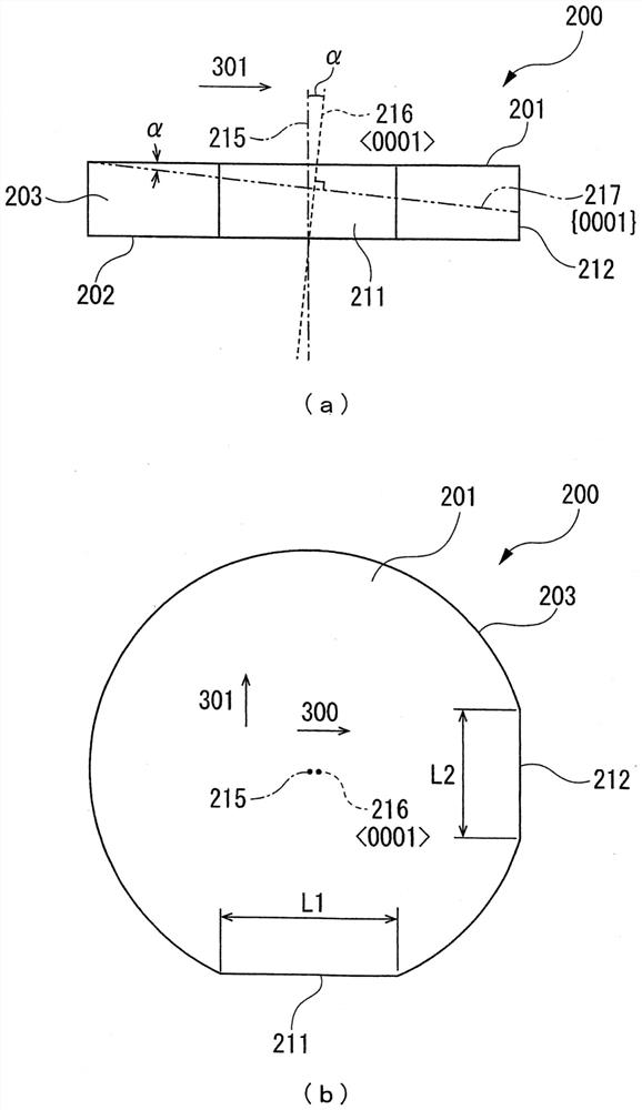
[0022] The wafer production method according to the embodiment of the present invention is a method of producing a wafer from a single crystal SiC ingot having a c-axis and a c-plane perpendicular to the c-axis. The wafer production method of the present embodiment includes a peeling layer formation step, a wafer production step, a separation step, and a cleaning step.

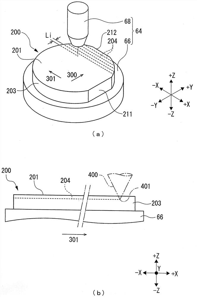
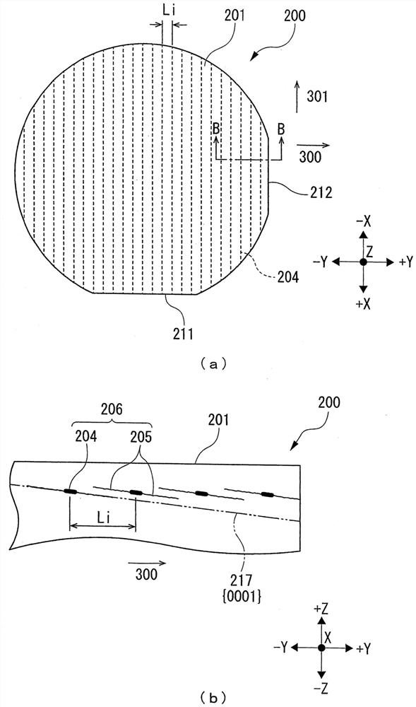
[0023] First, the structure of a single crystal SiC ingot will be described. Such as figure 1 As shown in (a), a single crystal SiC ingot (hereinafter simply referred to as an ingot) 200 is formed in a cylindrical shape as a whole. The ingot 200 has a flat first end surface 201 and a second end surface 202 opposite to the first end surface 201 . The first end surface 201 of the ingot 200 is an end surface irradiated with laser light. In addition, the peripheral surface 203 is located between the first end surface 201 and the second end surface 202 .

[0024] Such as figure 1 As shown in (a), the ingot 200...


PUM


Abstract

The invention provides a method for producing a wafer. The purpose of the present invention is to shorten the peeling time when a wafer is generated from the peeling of a SiC ingot. The wafer production method includes a wafer production step in which ultrasonic water is sprayed onto an end surface of an ingot on which a peeling layer is formed to peel the wafer from the ingot, thereby producing the wafer. Therefore, compared with a structure of simultaneously transmitting ultrasonic vibration to the whole end face of the ingot to strip the wafer, the stripping time can be shortened, and the ultrasonic water spraying nozzle and the ultrasonic vibration plate of the ultrasonic water spraying nozzle can be miniaturized. As a result, it is possible to achieve efficiency and cost reduction related to wafer peeling.

Description

technical field [0001] The present invention relates to methods of producing wafers. Background technique [0002] In the conventional techniques disclosed in Patent Documents 1 and 2, the SiC ingot is irradiated with laser light having a wavelength that is transparent to the SiC ingot. As a result, a peeling layer including a modified portion and a crack extending from the modified portion along the c-plane is formed at a portion at a depth corresponding to the thickness of the wafer from one surface of the SiC ingot. Furthermore, a SiC wafer is produced by delamination starting from the delamination layer. [0003] The peeling can be performed by transmitting ultrasonic vibrations to the peeling layer and connecting the peeling layers. In this way, in order to transmit the ultrasonic vibration to the peeling layer, after the peeling layer is formed, one surface of the SiC ingot is immersed in water, and the ultrasonic vibration oscillated from the ultrasonic vibration pl...

Claims


Application Information

Patent Timeline
Patent Type & Authority Applications(China)
IPC IPC(8): B28D5/04B28D5/00B23K26/53H01L21/02
CPCB28D5/047B28D5/0011B23K26/53H01L21/0201B26F3/004B26D7/086B23K2103/52B23K26/38B23K2101/40H01L21/02002B23K26/08H01L21/02052B08B3/02B08B3/12B28D5/0076B28D5/0094H01L29/1608
Inventor 邱晓明
Owner DISCO CORP
Why Eureka
Try Eureka