Digital Metasurface Based on Periodic Torus-Parabolic Composite Hole Arrays

A parabolic and periodic technology, applied in optical components, instruments, optics, etc., can solve problems such as crosstalk, increase system size, etc., achieve the effect of small size, convenient operation, and expansion of application sites and adaptable scope.

Active Publication Date: 2022-07-12
NANHUA UNIV
View PDF6 Cites 0 Cited by
  • Summary
  • Abstract
  • Description
  • Claims
  • Application Information

AI Technical Summary

Problems solved by technology

However, existing metasurface designs usually require auxiliary power and complex control circuits, which not only increase the size of the system, but also bring unfavorable crosstalk.

Method used


Image

  • Digital Metasurface Based on Periodic Torus-Parabolic Composite Hole Arrays
  • Digital Metasurface Based on Periodic Torus-Parabolic Composite Hole Arrays
  • Digital Metasurface Based on Periodic Torus-Parabolic Composite Hole Arrays

Examples


Embodiment 1

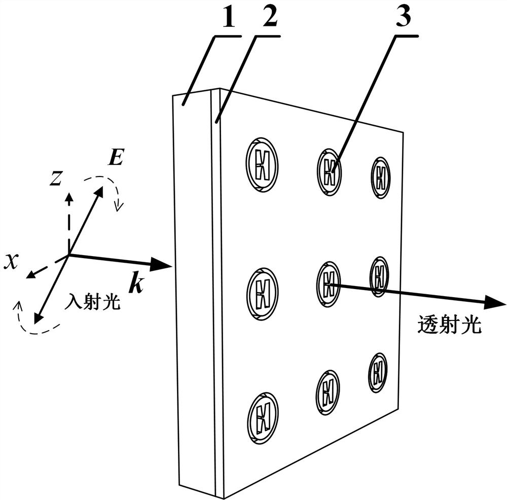
[0024] Example one, as Figure 1-4 As shown, a digital metasurface based on a periodic ring-parabolic composite hole array includes a dielectric substrate 1 and a metal thin film 2 , and the metal thin film 2 is disposed just above the dielectric substrate 1 .

[0025] The dielectric material of the dielectric substrate 1 is quartz, and the thickness of the quartz is 225 nm. The dielectric material of the dielectric substrate can also be any other dielectric suitable for processing, such as benzocyclobutene and the like.

[0026] The material of the metal thin film 2 is silver, and the thickness of the material silver of the metal thin film 2 is 50 nm. The material of the metal thin film 2 can also be other metals that can generate surface plasmons, such as gold and the like.

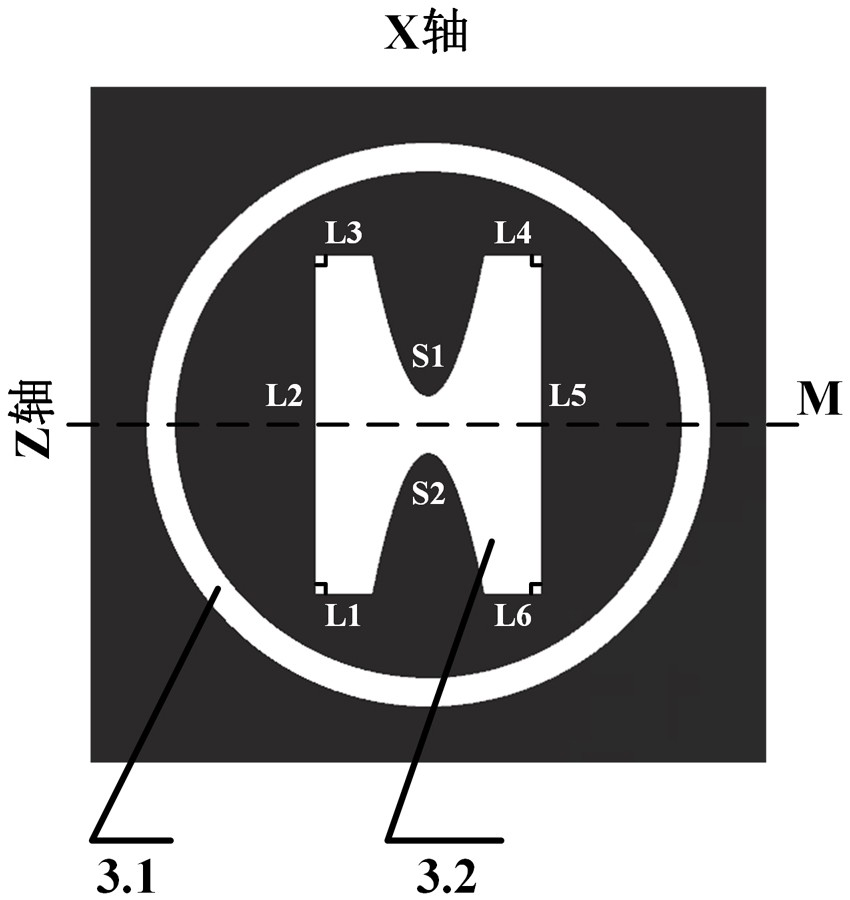
[0027] Nine ring-parabolic units 3 are etched on the metal film 2, and the nine ring-parabolic units 3 are arranged in a periodic array on the metal film 2. The nine ring-parabolic units 3 are 3×3 ar...

Embodiment 2

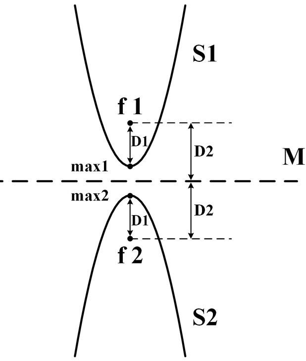
[0031] The second embodiment is similar in structure to the first embodiment, except that the dielectric material of the dielectric substrate 1 is quartz, the thickness of the quartz is 250 nm, the material of the metal thin film 2 is silver, and the thickness of the material silver of the metal thin film 2 is set. is 60 nm, the arrangement period of the ring-parabolic unit 3 is 300 nm, the inner radius of the ring 3.1 is 101 nm, and the width of the ring 3.1 is 23 nm, that is, the outer radius of the ring 3.1 is 124 nm. The length of the second straight side L2 of the parabolic hole 3.2 is equal to the length of the fifth straight side L5, and both are 140 nm. The lengths of the first straight side L1 , the third straight side L3 , the fourth straight side L4 and the sixth straight side L6 are equal to 25.5 nm. The distance D1 from the extreme points (vertices) max1 and max2 of the first parabolic side S1 and the second parabolic side S2 to the focal points f1 and f2 is 2.5 n...

Embodiment 3

[0032] The third embodiment is similar in structure to the first embodiment, except that the dielectric material of the dielectric substrate 1 is quartz, the thickness of the quartz is 350 nm, the material of the metal thin film 2 is silver, and the thickness of the silver of the material of the metal thin film 2 is set. is 150 nm, the arrangement period of the ring-parabolic unit 3 is 900 nm, the inner radius of the ring 3.1 is 250 nm, and the width of the ring 3.1 is 60 nm, that is, the outer radius of the ring 3.1 is 310 nm. The length of the second straight side L2 of the parabolic hole 3.2 is equal to the length of the fifth straight side L5, and both are 300 nm. The lengths of the first straight side L1 , the third straight side L3 , the fourth straight side L4 and the sixth straight side L6 are equal to 54.3 nm. The distance D1 from the extreme points (vertices) max1 and max2 of the first parabolic side S1 and the second parabolic side S2 to the focal points f1 and f2 i...


PUM

PropertyMeasurementUnit
thicknessaaaaaaaaaa
thicknessaaaaaaaaaa
radiusaaaaaaaaaa

Abstract

A digital metasurface based on a periodic ring-parabolic composite hole array, including a dielectric substrate and a metal film directly above it. A plurality of circular-parabolic units arranged in periodic arrays are etched on the metal film, and the circular-parabolic units include circular rings and parabolic holes that all run through the thickness direction of the metal film, and the parabolic holes are located in the circular ring and The center of the parabolic hole coincides with the center of the ring, and the parabolic hole is a symmetrical "H"-like structure, including a first parabolic side and a second parabolic side arranged axially symmetrically. By adjusting the polarization angle range of the incident light perpendicularly incident on the metal thin film from the direction of the dielectric substrate, an encodeable one-bit and two-bit transmission digital metasurface can be constructed. The invention has the advantages of simple structure, low requirements on manufacturing process, small size and convenient integration; high switching ratio, low power consumption, and no interference of pump light to signal light and subsequent optical paths.

Description

technical field [0001] The invention relates to the field of micro-nano photonic devices, in particular to a digital metasurface based on a periodic ring-parabolic composite hole array. Background technique [0002] In recent years, the modulation of the optical response of metasurfaces, especially the spectral response in the near-infrared region, remains a key challenge for the development of practical optical devices based on artificial digital metasurfaces. Artificial digital metasurfaces are usually composed of subwavelength artificial unit structures arranged periodically or quasi-periodically. The use of artificial digital metasurfaces can change the transmission characteristics of electromagnetic waves. Artificial digital metasurfaces are usually divided into transmissive electromagnetic metasurfaces and reflective electromagnetic metasurfaces. [0003] Existing various control mechanisms for metasurface design are mainly through the dynamic control of electromagnet...

Claims


Application Information

Patent Timeline
Patent Type & Authority Patents(China)
IPC IPC(8): G02B1/00G02B5/00
CPCG02B1/002G02B5/008
Inventor 王新林罗晓清欧杰骆又麟陈志勇朱卫华
Owner NANHUA UNIV
Why Eureka
Try Eureka