Epitaxial wafer of deep ultraviolet light emitting diode with bipolar AlN template layer
A technology of light-emitting diodes and template layers, applied in semiconductor devices, electrical components, circuits, etc., can solve the problems of high material difficulty, low carrier recombination efficiency, poor luminous efficiency of deep ultraviolet light-emitting diodes, etc., to improve luminous efficiency, The effect of promoting radiative recombination
- Summary
- Abstract
- Description
- Claims
- Application Information
AI Technical Summary
Problems solved by technology
Method used
Image

Examples
Embodiment Construction
[0035] In order to make the purpose, technical solution and advantages of the present disclosure clearer, the implementation manners of the present disclosure will be further described in detail below in conjunction with the accompanying drawings.
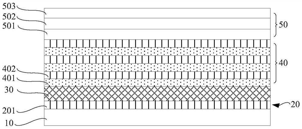
[0036] figure 1 It is a schematic structural diagram of an epitaxial wafer of a deep ultraviolet light-emitting diode with a bipolar AlN template layer provided by an embodiment of the present disclosure. Such as figure 1 As shown, the epitaxial wafer includes a substrate 10 and an AlN template layer 20 , an n-type AlGaN layer 30 , a multi-quantum well layer 40 and a p-type layer 50 sequentially formed on the substrate 10 .
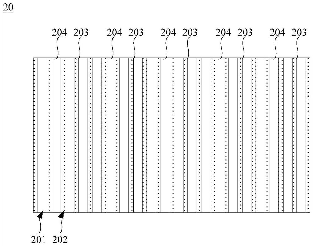
[0037] figure 2 is a schematic structural diagram of an AlN template layer provided by an embodiment of the present disclosure. Such as figure 2 As shown, the surface of the AlN template layer 20 away from the substrate 10 has a plurality of first polarity regions 203 and a plurality of second polarity r...
PUM
| Property | Measurement | Unit |
|---|---|---|
| Width | aaaaa | aaaaa |
| Thickness | aaaaa | aaaaa |
| Thickness | aaaaa | aaaaa |
Abstract
Description
Claims
Application Information
 - R&D
- Intellectual Property
- Life Sciences
- Materials
- Tech Scout
- Unparalleled Data Quality
- Higher Quality Content
- 60% Fewer Hallucinations
Browse by: Latest US Patents, China's latest patents, Technical Efficacy Thesaurus, Application Domain, Technology Topic, Popular Technical Reports.
© 2025 PatSnap. All rights reserved.Legal|Privacy policy|Modern Slavery Act Transparency Statement|Sitemap|About US| Contact US: help@patsnap.com