3DIC chip and preparation method of 3DIC chip

A chip and chip body technology, applied in semiconductor/solid-state device manufacturing, electrical components, electrical solid-state devices, etc., can solve the problems of bump stress concentration, stress concentration, unevenness, etc., to avoid the risk of virtual welding and ensure coplanarity. degree of effect

Pending Publication Date: 2021-11-09
XI AN UNIIC SEMICON CO LTD
View PDF0 Cites 1 Cited by
  • Summary
  • Abstract
  • Description
  • Claims
  • Application Information

AI Technical Summary

Problems solved by technology

[0006] In order to solve the technical problem of stress concentration and unevenness caused by bumps in the existing 3DIC chip, the invention provides a 3DIC chip and a method for preparing the 3DIC chip
Solve the problems of stress concentration and unevenness by adding virtual bumps

Method used


Image

  • 3DIC chip and preparation method of 3DIC chip
  • 3DIC chip and preparation method of 3DIC chip
  • 3DIC chip and preparation method of 3DIC chip

Examples


Embodiment 1

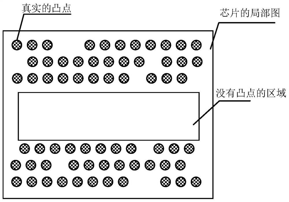
[0049] The present invention provides a 3DIC chip, comprising: a chip body, a window is opened on the first surface of the chip body; Staggered; the top metal layer is set under the first surface; the chip pad is set on the top metal layer, and the real bump is set on the chip pad. Disposing the real bumps on the chip pads can ensure the signal transmission capability of the real bumps, and the dummy bumps are disposed on the first surface to distribute stress but not transmit signals.

Embodiment 2

[0051] In order to reduce the height difference between the real bump and the dummy bump and prevent oxidation of the metal layer of the chip, a passivation layer is provided. On the basis of Embodiment 1, a passivation layer is also included. The passivation layer is disposed on the first surface, the sidewall of the window and covers the top metal layer without chip pads; the dummy bump is disposed on the passivation layer corresponding to the first surface. The passivation layer completely covers the bare top metal layer and the first surface to prevent oxidation of the metal layer. The virtual bumps are set on the passivation layer, the real bumps are set on the chip pads, the virtual bumps and the real bumps grow at the same time, and the height difference between the virtual bumps and the real bumps is only the upper surface of the chip pad and the The distance between the top surfaces of the passivation layer.

Embodiment 3

[0053]In order to reduce the stress of the passivation layer, a transition layer is covered on the passivation layer and fills the opening. The transition layer is generally a polymer. The dummy bumps can be disposed on the passivation layer as described in Embodiment 2, and grow through the transition layer. The real bumps are placed on the die pads, also through the transition layer. Dummy bumps can also be placed directly on the transition layer. However, although the direct setting of virtual bumps on the transition layer can also solve the problem of stress concentration, the welding accuracy must be well controlled. If the height difference between the virtual bumps and the real bumps exceeds the tolerance requirements for chip flipping, cause solder joint problems.

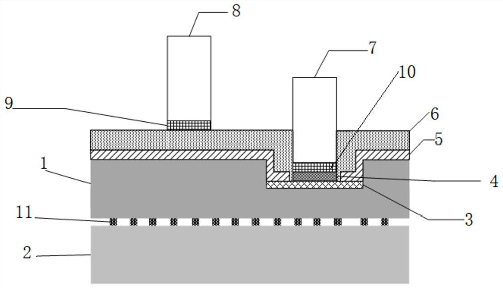
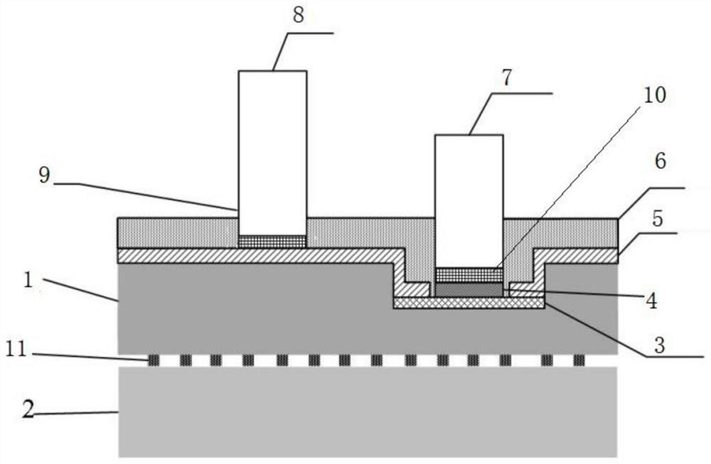
[0054] The specific structure is as figure 2 As shown, a 3DIC chip includes a chip body, a top metal layer, a metal layer, a passivation layer, and a polymer layer (ie, a transition layer). The chip bo...


PUM


Abstract

The invention relates to a 3DIC chip and a preparation method of the 3DIC chip. The 3DIC chip comprises a chip body which is provided with a window in a first surface thereof; a first bump which is arranged in the window; and a second bump which is arranged on the first surface of the chip body and staggered from the window in position. The first bump is used for transmitting signals, the second bump is used for dispersing stress of the first bump, and the height difference between the first bump and the second bump is smaller than or equal to a threshold. According to the invention, the technical problem of stress concentration and non-uniformity caused by bumps in the existing 3DIC chip is solved, the height difference between the first bump and the second bump is ensured to be within a predetermined range, the coplanarity of a virtual bump and a real bump is ensured, and the cold solder joint risk during flip chip mounting is avoided.

Description

technical field [0001] The invention belongs to the field of 3DIC chip packaging, and in particular relates to a 3DIC chip and a preparation method for the 3DIC chip. Background technique [0002] Bonding technology is an important basis for 3D integration technology. Bonding technologies mainly include dielectric bonding, hybrid bonding (Hybrid Bonding), metal bonding, etc. Among them, hybrid bonding can complete the electrical connection between wafers while realizing wafer bonding, reducing the electrical connection after bonding. Connection process, high bonding efficiency. The current 3DIC hybrid bonding technology is a wafer-level electrical connection technology developed on the basis of CMOS image sensors in recent years. The specific process is: 1) Select a wafer with appropriate capacity, bit width, and interface rate; 2) Different wafers use their own process tape-out; 3) After planarizing the top layer metal of each wafer, grow Cu bonding pillars; 4) Turn the w...

Claims


Application Information

Patent Timeline
Patent Type & Authority Applications(China)
IPC IPC(8): H01L21/60H01L23/488H01L25/065
Inventor 王慧梅
Owner XI AN UNIIC SEMICON CO LTD
Why Eureka
Try Eureka