P-type electron barrier layer structure, LED epitaxial structure and preparation method thereof

An electron blocking layer and epitaxial structure technology, applied in circuits, electrical components, semiconductor devices, etc., can solve problems such as lattice mismatch and excessive stress, reduce distortion, improve lattice mismatch, and improve LED luminescence. Efficiency and effect of antistatic properties

Pending Publication Date: 2021-11-23
广州市众拓光电科技有限公司
View PDF0 Cites 0 Cited by
  • Summary
  • Abstract
  • Description
  • Claims
  • Application Information

AI Technical Summary

Problems solved by technology

It can improve the problems of lattice mismatch and excessive stress between the electron blocking layer and the P-type GaN layer, thereby improving the luminous efficiency and antistatic performance of the LED

Method used


Image

  • P-type electron barrier layer structure, LED epitaxial structure and preparation method thereof
  • P-type electron barrier layer structure, LED epitaxial structure and preparation method thereof
  • P-type electron barrier layer structure, LED epitaxial structure and preparation method thereof

Examples


Embodiment 1

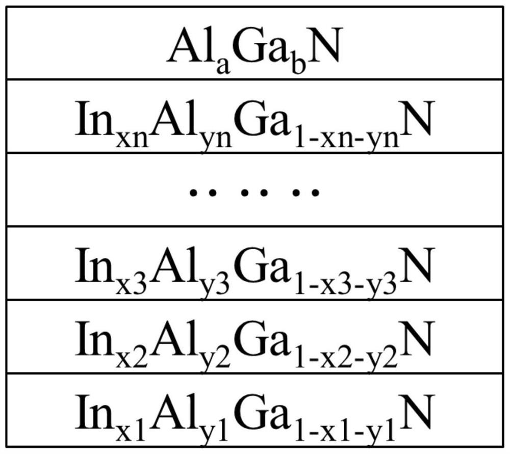
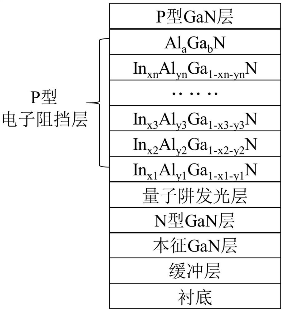
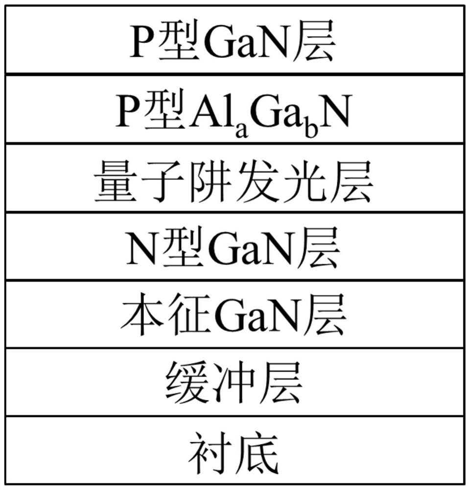
[0036] An LED epitaxial structure, including a substrate, a buffer layer, an intrinsic GaN layer, an N-type GaN layer, a quantum well light-emitting layer, a P-type electron blocking layer, and a P-type GaN layer from bottom to top; wherein, the P-type electron blocking layer structure , including P-type In with a cycle number of n=2 from bottom to top xn Al yn Ga 1-xn-yn N-layer and P-type Al a Ga b N layer; that is, the P-type electron blocking layer structure includes P-type In from bottom to top 0.1 Al 0.1 Ga 0.8 N layer, P type In 0.05 Al 0.15 Ga 0.8 N-layer and P-type Al 0.2 Ga 0.8 N layer; P-type Al a Ga b In the N layer, a=0.2, b=0.8.

[0037] The preparation method of the LED epitaxial structure comprises the following steps:

[0038] Step S1: prepare a substrate, and grow a buffer layer on the substrate; the growth temperature of the buffer layer is 950° C., the growth thickness is 500 nm, and the growth pressure is 100 Torr;

[0039] Step S2: growing ...

Embodiment 2

[0045] An LED epitaxial structure, including a substrate, a buffer layer, an intrinsic GaN layer, an N-type GaN layer, a quantum well light-emitting layer, a P-type electron blocking layer, and a P-type GaN layer from bottom to top; wherein, the P-type electron blocking layer structure , including P-type In with period number n=4 from bottom to top xn Al yn Ga 1-xn-yn N-layer and P-type Al a Ga b N layer; that is, the P-type electron blocking layer structure includes P-type In from bottom to top 0.1 Al 0.1 Ga 0.8 N layer, P type In 0.08 Al 0.12 Ga 0.8 N layer, P type In 0.06 Al 0.14 Ga 0.8 N layer, P type In 0.04 Al 0.16 Ga 0.8 N layer and P-type AlGaN layer; P-type Al a Ga b In the N layer, a=0.2, b=0.8.

[0046] The preparation method of the LED epitaxial structure comprises the following steps:

[0047] Step S1: prepare a substrate, and grow a buffer layer on the substrate; the growth temperature of the buffer layer is 950° C., the growth thickness is 500 ...

Embodiment 3

[0054] An LED epitaxial structure, including a substrate, a buffer layer, an intrinsic GaN layer, an N-type GaN layer, a quantum well light-emitting layer, a P-type electron blocking layer, and a P-type GaN layer from bottom to top; wherein, the P-type electron blocking layer structure , including P-type In with period number n=5 from bottom to top xn Al yn Ga 1-xn-yn N-layer and P-type Al a Ga b N layer; that is, the P-type electron blocking layer structure includes P-type In from bottom to top 0.12 Al 0.08 Ga 0.8 N layer, P type In 0.1 Al 0.1 Ga 0.8 N layer, P type In 0.08 Al 0.12 Ga 0.8 N layer, P type In 0.06 Al 0.14 Ga 0.8 N layer, P type In 0.04 Al 0.16 Ga 0.8 N layer and P-type AlGaN layer; P-type Al a Ga b In the N layer, a=0.2, b=0.8.

[0055] The preparation method of the LED epitaxial structure comprises the following steps:

[0056] Step S1: prepare a substrate, and grow a buffer layer on the substrate; the growth temperature of the buffer laye...


PUM

PropertyMeasurementUnit
thicknessaaaaaaaaaa
thicknessaaaaaaaaaa
thicknessaaaaaaaaaa

Abstract

The invention relates to the technical field of light emitting diodes, in particular to a P-type electron barrier layer structure, an epitaxial structure and a preparation method thereof. The P-type electron barrier layer structure comprises a multi-cycle P-type In<xn>Al<yn>Ga< 1-xn-n-yn>N layer and a P-type AlGaN layer from bottom to top, wherein n is greater than 1 and less than or equal to 6. The LED epitaxial structure comprises a substrate, a buffer layer, an intrinsic GaN layer, an N-type GaN layer, a quantum well light-emitting layer, the P-type electron barrier layer and a P-type GaN layer from bottom to top. The P-type electron barrier layer structure and the LED epitaxial structure provided by the invention can adjust stress, improve lattice mismatch of a material interface, reduce distortion of an energy band of a light-emitting layer, improve electron and hole recombination efficiency, and improve light-emitting efficiency and antistatic performance of an LED.

Description

technical field [0001] The invention relates to the technical field of light-emitting diodes, in particular to a P-type electron blocking layer structure and its LED epitaxial structure and preparation method. Background technique [0002] Light-emitting diode (LED) is a commonly used light-emitting device, which releases energy and emits light through the recombination of electrons and holes. It is widely used in the field of lighting. Light-emitting diodes can efficiently convert electrical energy into light energy, and have a wide range of uses in modern society, such as lighting, flat panel displays, medical devices, etc. With the continuous development of LED technology, while it is being used more and more widely, it is also facing higher and higher requirements, especially the luminous efficiency and antistatic performance of LED. [0003] At present, the luminous efficiency of LED is still not high, especially with the reduction of chip size and the increasing curre...

Claims


Application Information

Patent Timeline
Patent Type & Authority Applications(China)
IPC IPC(8): H01L33/14H01L33/12H01L33/00
Inventor 李国强
Owner 广州市众拓光电科技有限公司
Why Eureka
Try Eureka