Packaging structure and optical module

A packaging structure and packaging substrate technology, which is applied in the field of optical communication, can solve the problems of reducing the optical bandwidth and affecting the quality of high-frequency signal transmission, and achieve the effects of improving the optical bandwidth, reducing coupling, and good high-frequency performance

Active Publication Date: 2021-11-23
INNOLIGHT TECHNOLOGY (SUZHOU) LTD
View PDF5 Cites 0 Cited by
  • Summary
  • Abstract
  • Description
  • Claims
  • Application Information

AI Technical Summary

Problems solved by technology

The one-piece structural design in which the matching resistor 30' and the filter capacitor 40' are integrated into the packaging substrate 10' improves the degree of integration and reduces the volume of the optical module, but due to the link between the matching resistor 30' and the filter capacitor 40' and The ground metal GND 11' is on the same surface, and coupling between the link of the matching resistor 30' and the filter capacitor 40' and the ground metal GND 11' is easy to occur, which affects the quality of high-frequency signal transmission and reduces the photoelectric bandwidth

Method used


Image

  • Packaging structure and optical module
  • Packaging structure and optical module
  • Packaging structure and optical module

Examples


Embodiment 1

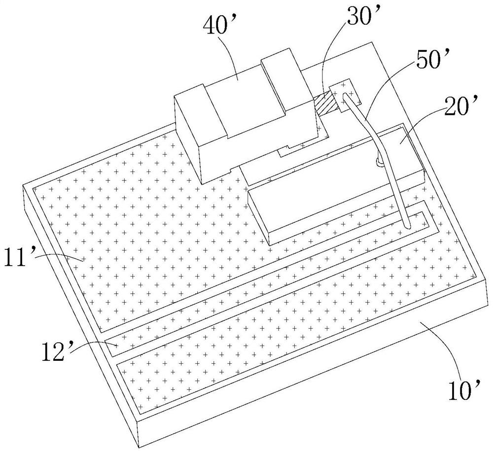
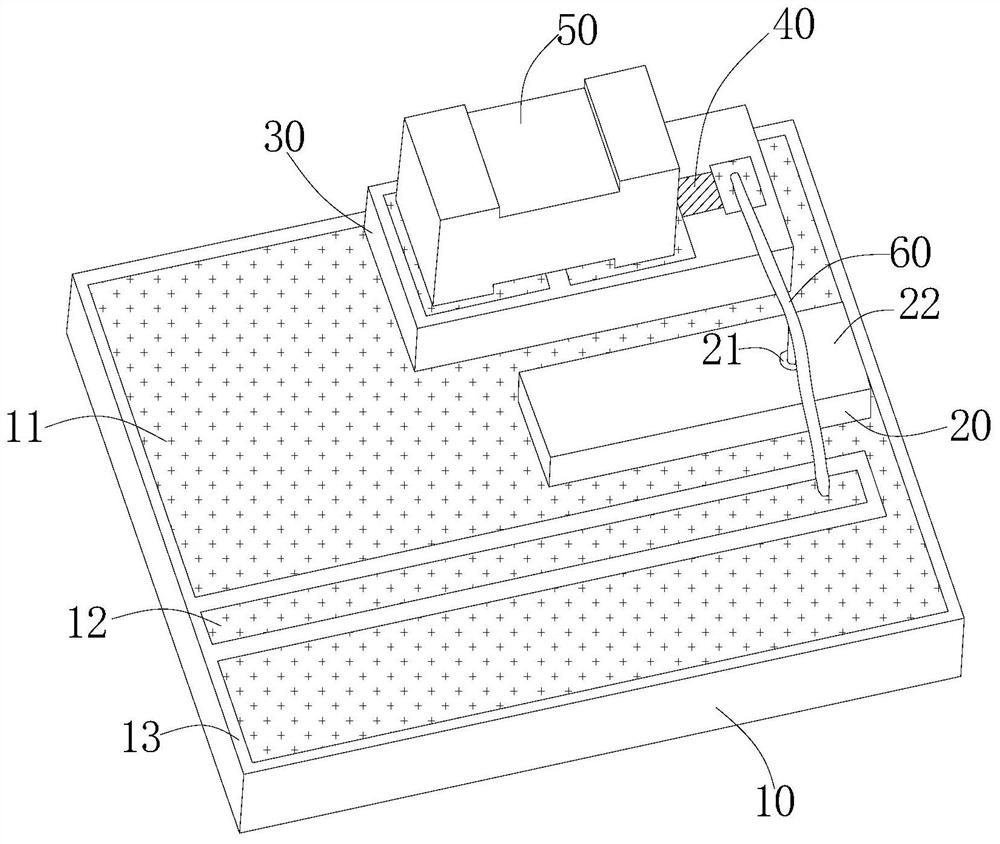
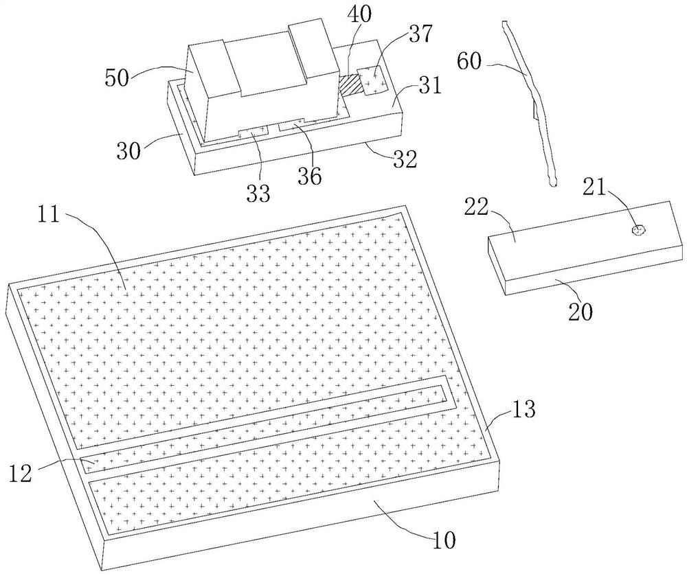
[0037] Such as Figure 2-4 As shown, this embodiment provides a COC (chip on ceramic, chip on ceramic substrate) packaging structure, including a packaging substrate 10 and at least one semiconductor laser chip 20 and at least one sub-substrate disposed on the packaging substrate 10 30 and a matching circuit. In this embodiment, there is a single semiconductor laser chip 20 and a single sub-substrate 30 on the package substrate 10 . A ground metal 11 and at least one signal line 12 are provided on the package substrate 10 , here, corresponding to a single semiconductor laser chip 20 , a single signal line 12 is provided on the package substrate 10 . In this embodiment, the upper surface of the packaging substrate 10 has a metal layer, and the signal line is formed on the metal layer to form the ground metal 11 and the signal line 12 with a coplanar line structure on the upper surface of the packaging substrate 10. Here, the packaging The upper surface of the substrate 10 is t...

Embodiment 2

[0041] Such as Image 6 As shown, the difference from Embodiment 1 is that in this embodiment, the above-mentioned packaging substrate 10 is provided with a first upper surface 13 and a second upper surface 14, and the signal line 12 and the semiconductor laser chip 20 of the packaging substrate 10 are arranged on the second upper surface. On the first upper surface 13 , the sub-substrate 30 is disposed on the second upper surface 14 , wherein the height of the second upper surface 14 is lower than that of the first upper surface. Here, the first upper surface 13 is the same as the upper surface of the package substrate in Embodiment 1, and has the signal line 12 and the ground metal 11 with a coplanar line structure. Specifically, a stepped plane is made on the side of the packaging substrate 10 away from the signal line 12 as the second upper surface 14, and the second upper surface 14 is lower than the first upper surface 13 of the packaging substrate 10, so that the device...

Embodiment 3

[0044] Such as Figure 7 As shown, the difference from Embodiment 2 is that in this embodiment, the packaging substrate 10 is also provided with a third upper surface 15, that is, the packaging substrate 10 is provided with a first upper surface 13, a second upper surface 14 and a third upper surface. Surface 15. Wherein, the height of the second upper surface 14 is lower than that of the third upper surface 15 , and the height of the third upper surface 15 is lower than that of the first upper surface 13 . Here, the first upper surface 13 is the same as the upper surface of the package substrate in Embodiment 1, and has a signal line 12 and a ground metal 11 with a coplanar line structure, the sub-substrate 30 is arranged on the second upper surface 14, and the semiconductor laser 20 is arranged on the second upper surface 14. on the third upper surface 15 . In this embodiment, the third upper surface 15 is located between the second upper surface 14 and the signal line 12,...


PUM


Abstract

The invention discloses a packaging structure and an optical module. The packaging structure comprises a packaging substrate, at least one semiconductor laser chip, at least one sub-substrate and a matching circuit, wherein the semiconductor laser chip and the sub-substrate are arranged on the packaging substrate, and at least part of the matching circuit is arranged on the sub-substrate; the semiconductor laser chip is provided with a signal electrode, the packaging substrate is provided with grounding metal and at least one signal line, and the at least one signal line is electrically connected with the signal electrode of the laser chip; the matching circuit comprises an input end, at least one electronic element and a grounding end; and the input end is electrically connected with the signal electrode of the laser chip, the two ends of at least one electronic element are electrically connected with the input end and the grounding end respectively, and the grounding end is electrically connected with the grounding metal of the packaging substrate. The sub-substrate is additionally arranged on the packaging substrate and used for designing laser matching circuits such as an RC circuit, so that coupling between a matching resistor and the GND and coupling between a filtering capacitor and the GND are reduced, the photoelectric bandwidth is improved, and good high-frequency performance is achieved.

Description

technical field [0001] The present application relates to the technical field of optical communication, in particular to a packaging structure and an optical module. Background technique [0002] The laser chip in the optical module mostly adopts the packaging design of COC (chip on ceramic, chip on ceramic substrate). The commonly used structure is as follows: figure 1 As shown, coplanar lines including ground metal 11' and signal lines 12' are designed on the package substrate 10', and the semiconductor laser chip 20' is mounted on the package substrate 10'. In order to reduce the volume of the optical module, the matching circuit of the laser, such as the filter capacitor 40' and the matching resistor 30', is generally integrated on the above-mentioned packaging substrate 10', and the semiconductor laser chip 20' is connected to the matching resistor 30' through a gold wire 50' , the matching resistor 30' is connected to the ground metal (GND) 11' through the filter capa...

Claims


Application Information

Patent Timeline
Patent Type & Authority Applications(China)
IPC IPC(8): H01S5/0233H01S5/02345
CPCH01S5/0206H01S5/02345
Inventor 贾秀红汪振中
Owner INNOLIGHT TECHNOLOGY (SUZHOU) LTD
Why Eureka
Try Eureka