
Photoresist baking apparatus

A technology of baking equipment and photoresist, which is applied in the fields of opto-mechanical equipment, optics, and photosensitive material processing to achieve the effect of uniform film morphology

Pending Publication Date: 2021-11-26
TAIWAN SEMICON MFG CO LTD
View PDF0 Cites 2 Cited by
  • Summary
  • Abstract
  • Description
  • Claims
  • Application Information

AI Technical Summary

Problems solved by technology

[0004] Although existing photoresist baking equipment has been adequate for its intended purpose, they are not completely satisfactory in all respects

Method used


Image

  • Photoresist baking apparatus
  • Photoresist baking apparatus
  • Photoresist baking apparatus

Examples


Embodiment Construction

[0047] The following disclosure provides many different embodiments or examples for implementing different features of the present invention. Examples of specific components and their arrangements are described below to illustrate the present disclosure. Of course, these embodiments are only examples, which should not limit the scope of the present disclosure. For example, it is described in the specification that a first feature is formed on or over a second feature, which may include an embodiment in which the first feature is in direct contact with the second feature, and may also include an embodiment in which additional features are formed on the first feature. An embodiment between a feature and a second feature such that the first feature and the second feature may not be in direct contact. In addition, repeated reference symbols and / or signs may be used in different examples of the present disclosure. This repetition is for the purpose of simplicity and clarity, and i...


PUM


Abstract

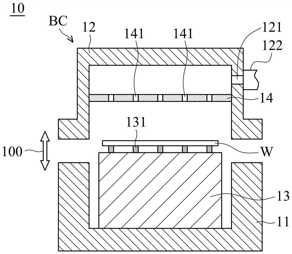
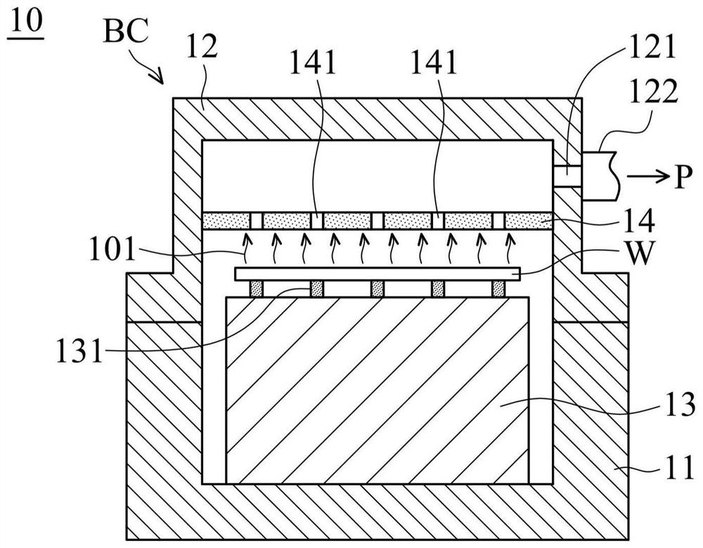
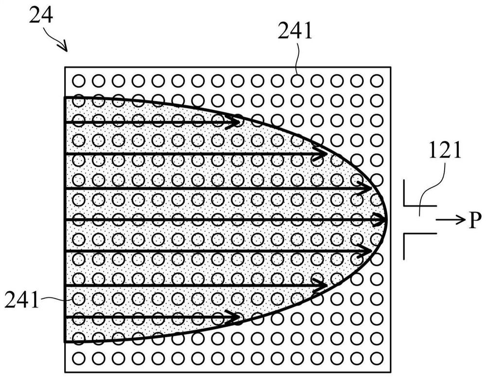
The embodiments of the invention provides a photoresist baking apparatus. The photoresist baking apparatus includes a baking chamber, a hot plate, an exhaust line, and a cover plate. The baking chamber has an exhaust port on a sidewall thereof. The hot plate is disposed in the baking chamber and is configured to support a wafer and heat a photoresist material over the wafer. The exhaust line is coupled to the exhaust port and is configured to exhaust out the atmosphere inside the baking chamber. The cover plate is disposed over the hot plate and between the hot plate and the exhaust port. The cover plate has multiple exhaust holes to allow air to flow through. The size of one of the exhaust holes farther from the exhaust port is larger than the size of one of the exhaust holes closer to the exhaust port.

Description

technical field [0001] Embodiments of the present invention relate to a photoresist baking equipment, in particular to a photoresist baking equipment with a cover plate that can improve the airflow field distribution of a baking chamber. Background technique [0002] Semiconductor devices are used in various electronic applications such as personal computers, cell phones, digital cameras, and other electronic equipment. In general, semiconductor devices are fabricated by sequentially depositing materials for insulating or dielectric layers, conductive layers, and semiconductor layers on a semiconductor substrate (such as a wafer), and patterning the various material layers using a photolithography process to Circuit components and elements are formed thereon. [0003] Photolithography is a process that uses light-sensitive photoresist materials and produces circuit patterns on the surface of wafers under controlled exposure to light. Applying and developing photoresist inv...

Claims


Application Information

Patent Timeline
IPC IPC(8): G03F7/38G03F7/40
CPCG03F7/38G03F7/40G03F7/168H01L21/6715H01L21/67109H01L21/6875
Inventor 陈柏宏陈裕凯
Owner TAIWAN SEMICON MFG CO LTD
Learn More