Supercharge Your Innovation With Domain-Expert AI Agents!

OTP memory array and read-write method

A technology of memory array and read-write method, applied in static memory, read-only memory, information storage, etc., can solve the problems of Vt voltage drop loss, large Vt voltage drop loss, and high read voltage, so as to reduce leakage current and simplify translation The effect of encoder design and easy programming

Active Publication Date: 2021-11-26
CHENGDU KILOWAY ELECTRONICS CO LTD
View PDF7 Cites 0 Cited by
  • Summary
  • Abstract
  • Description
  • Claims
  • Application Information

AI Technical Summary

Problems solved by technology

[0008] figure 1 , figure 2 , image 3 There is a problem of Vt voltage drop loss caused by capacitor C0, MOS tube M3, MOS tube M4, etc.
[0009] figure 1 , figure 2 , image 3 , Figure 4 structure, the word line requires a larger area of ​​high-voltage decoding circuit, and the word line also requires a larger area of ​​3V medium voltage decoding circuit, while the word line has to handle high-low dual voltage switching, and the bit line has to handle medium-low Dual-voltage switching, the resulting design complexity of various voltage combinations, the risk of leakage caused by insufficient verification coverage, and numerous level-shifting interface circuits
[0010] also, figure 1 , figure 2 , image 3 , Figure 4 The peripheral circuit also has the problem of large Vt voltage drop loss and high read voltage due to the use of thick gate oxide devices (Vt is usually high, >0.7V) in the medium and high voltage paths.

Method used


Image

  • OTP memory array and read-write method
  • OTP memory array and read-write method
  • OTP memory array and read-write method

Examples


Embodiment 1

[0043] see Figure 5 , this embodiment includes a storage MOS transistor C0, a first MOS transistor M1, a second MOS transistor M2 and a detection MOS transistor M0, one current connection end of the first MOS transistor M1 is connected to the first current connection end of the detection MOS transistor M0, The control terminal of the detection MOS transistor M0 is connected to a current connection point of the second MOS transistor M2, the control terminal of the detection MOS transistor M0 is also connected to the storage MOS transistor C0, and a control terminal of the detection MOS transistor M0 and the storage MOS transistor C0 is provided. isolation module,

[0044] The storage MOS transistor C0 is a Native MOS transistor, and the isolation module is a Native MOS transistor M3.

Embodiment 2

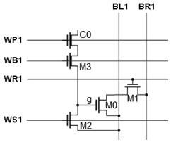
[0046] see Image 6 , this embodiment includes a storage MOS transistor C0, a first MOS transistor M1, a second MOS transistor M2 and a detection MOS transistor M0, one current connection end of the first MOS transistor M1 is connected to the first current connection end of the detection MOS transistor M0, The control terminal of the detection MOS transistor M0 is connected to a current connection point of the second MOS transistor M2, the control terminal of the detection MOS transistor M0 is also connected to the storage MOS transistor C0, and a control terminal of the detection MOS transistor M0 and the storage MOS transistor C0 is provided. isolation module,

[0047] The storage MOS tube C0 is a Native MOS tube, and the isolation module is composed of two Native MOS tubes connected in series, see Image 6 Native MOS tubes shown in M3 and M4.

Embodiment 3

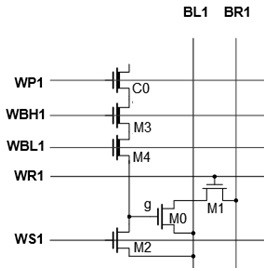
[0049] see Figure 7 , this embodiment includes a storage MOS transistor C0, a first MOS transistor M1, a second MOS transistor M2 and a detection MOS transistor M0, one current connection end of the first MOS transistor M1 is connected to the first current connection end of the detection MOS transistor M0, The control terminal of the detection MOS transistor M0 is connected to a current connection point of the second MOS transistor M2, the control terminal of the detection MOS transistor M0 is also connected to the storage MOS transistor C0, and a control terminal of the detection MOS transistor M0 and the storage MOS transistor C0 is provided. isolation module,

[0050] The storage MOS transistor C0 is a Native MOS transistor, and the isolation module is composed of at least three Native MOS transistors connected in series.


PUM


Abstract

The invention discloses an OTP memory array and a read-write method, and relates to an integrated circuit technology. An OTP memory array is composed of M*N OTP memories, each OTP memory comprises a storage MOS transistor, a first MOS transistor, a second MOS transistor and a detection MOS transistor, and an isolation module is arranged between a control end of the detection MOS transistor and the storage MOS transistor; the storage MOS transistor is a Native MOS transistor, and both M and N are integers greater than 1; the isolation module is composed of at least one isolation MOS transistor, and the isolation MOS transistor is a Native MOS transistor. In the array, the grid electrodes of the storage MOS transistors are connected to a same storage control point, the isolation MOS transistors are distinguished according to the distance values from the MOS transistors, and the grid electrodes of the isolation MOS transistors with the same distance value are connected to a same isolation control point. According to the present invention, the leakage current can be greatly reduced, and the programming effect is improved.

Description

technical field [0001] The present invention relates to integrated circuit technology and OTP memory technology. Background technique [0002] Figure 1~Figure 4 4 prior art are shown, figure 1 For the XLPM memory cell prototype, figure 2 is an XLPM memory cell with a read isolation device, image 3 It is an XLPM memory cell with a high-voltage isolation device, Figure 4 It is an XLPM memory cell using NativeMOS gate capacitance. [0003] by figure 1 The XLPM memory cells shown are based on the figure 2 Adding the read isolation device M1 can isolate the crosstalk between the memory cells located on the common bit lines BL and BR. Moreover, due to the isolation function of this device, it is no longer necessary to perform the clearing operation of all cells, but only need to perform the clearing operation on the memory cells on the word line to be read, thereby reducing the power consumption caused thereby. [0004] image 3 A high-voltage isolation device with ...

Claims


Application Information

Patent Timeline
Patent Type & Authority Applications(China)
IPC IPC(8): G11C17/18G11C5/06G11C5/14
CPCG11C17/18G11C5/063G11C5/145G11C17/16G11C7/1069G11C7/20
Inventor 彭泽忠毛军华
Owner CHENGDU KILOWAY ELECTRONICS CO LTD
Features
  • R&D
  • Intellectual Property
  • Life Sciences
  • Materials
  • Tech Scout
  • Unparalleled Data Quality
  • Higher Quality Content
  • 60% Fewer Hallucinations
Learn More