Three-dimensional quantum chip and preparation method thereof

A quantum and three-dimensional technology, applied in the field of multi-qubit chips, can solve the problems of difficult wiring, difficult to achieve wiring, and harsh requirements for pins, and achieve the effect of improving energy relaxation time, easy large-scale expansion, and eliminating preparation problems.

Pending Publication Date: 2021-11-30
INST OF PHYSICS - CHINESE ACAD OF SCI
View PDF8 Cites 0 Cited by
  • Summary
  • Abstract
  • Description
  • Claims
  • Application Information

AI Technical Summary

Problems solved by technology

For the first method, wiring for 50-100 qubits can be achieved, but for larger quantities, wiring is very difficult
The larger the number of qubits, the longer the wiring, which greatly reduces the yield during preparation
For the second method, the pins are in contact with the chip, which is likely to cause heat, strain, and easily damage the chip, and the production of the pins is also demanding, including problems such as the force on the pins and the alignment of the pins during contact.
Therefore, using the above method to prepare a chip with hundreds or thousands of qubits not only requires a lot of work but also makes wiring difficult.

Method used


Image

  • Three-dimensional quantum chip and preparation method thereof
  • Three-dimensional quantum chip and preparation method thereof
  • Three-dimensional quantum chip and preparation method thereof

Examples


Embodiment 1

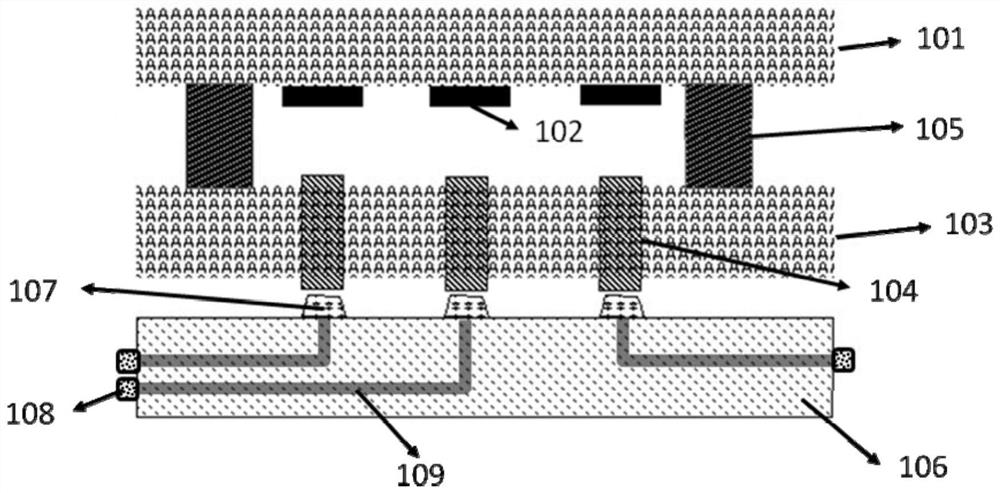
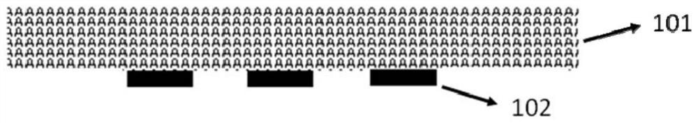
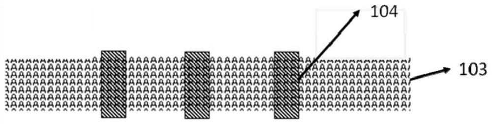
[0041] figure 1 It is a schematic cross-sectional view of a three-dimensional quantum chip prepared in an embodiment of the present invention. Such as figure 1 As shown, the three-dimensional quantum chip includes a qubit layer, an auxiliary graphics layer and a wiring layer. Wherein, the qubit layer includes a substrate 101 and qubits 102 prepared on the substrate 101 . The auxiliary pattern layer includes a substrate 103, various auxiliary patterns prepared on the substrate 103, and through holes 104 penetrating the substrate 103 and deposited with metal. The wiring layer can be a PCB board 106 , inside the PCB board 106 there are a plurality of connection wires 109 , one end of which is connected to the connection terminal 107 , and the other end is connected to the joint 108 . Preferably, the connecting terminals 107 are located on the surface of the PCB 106 facing the side of the auxiliary graphics layer. The connector 108 may be a sma or smp connector for interfacing...

Embodiment 2

[0063] Figure 7 It is a schematic cross-sectional view of a three-dimensional quantum chip prepared in another embodiment of the present invention. Such as Figure 7 As shown, the three-dimensional quantum chip includes a qubit layer, an auxiliary graphics layer and a wiring layer. Wherein, the qubit layer includes a substrate 101 and qubits 102 prepared on the substrate 101 . The auxiliary pattern layer includes a substrate 103, various auxiliary patterns prepared on the substrate 103, and through holes 104 penetrating the substrate 103 and deposited with metal. The wiring layer can be a PCB board, and the PCB board 106 has a plurality of connection wires 109 inside, one end of which is connected to the connection terminal 110 , and the other end is connected to the connector 108 . Preferably, the connecting terminal 110 is located on the surface of the side of the PCB 106 facing away from the auxiliary graphics layer. The connector 108 may be a sma or smp connector for ...


PUM


Abstract

The invention provides a three-dimensional quantum chip, which comprises a quantum bit layer, an auxiliary pattern layer and a wiring layer, wherein the quantum bit layer comprises a first substrate and quantum bits on the first substrate; the auxiliary pattern layer comprises a second substrate, a plurality of auxiliary patterns on the second substrate and a through hole which penetrates through the second substrate and is deposited with metal; the wiring layer comprises a connecting line and a connecting terminal, the first end of the connecting line is connected to the connecting terminal, and the second end of the connecting line is used for outputting data; and the surface, which is provided with the quantum bits, of the quantum bit layer and the surface, which is provided with the auxiliary patterns, of the auxiliary pattern layer are welded together through connecting metal, and the connecting terminal on the wiring layer is connected with the deposited metal in the through hole in the surface of the auxiliary pattern layer without the auxiliary patterns.

Description

technical field [0001] The present invention generally relates to the field of multi-qubit chips, and in particular to a three-dimensional quantum chip and a preparation method thereof. Background technique [0002] The three-dimensional quantum chip is a semiconductor process that uses flip-chip packaging technology to weld two or more chips together upside down. Using this process in the preparation of quantum chips can solve problems such as large crosstalk, difficult integration, and complicated wiring. At present, there are mainly two methods for the preparation of three-dimensional quantum chips. One method is to align the quantum chip with the bit layer with the chip with the wiring layers such as transmission lines, readout chambers, and various control lines through the form of alignment and flipping. Realize a three-dimensional quantum chip (see B.Foxen, et.al.2018Quantum Sci.Technol.3, 014005); another method is to use pins to contact the pins of the leads on the ...

Claims


Application Information

Patent Timeline
Patent Type & Authority Applications(China)
IPC IPC(8): H01L25/16H01L23/488H01L21/50
CPCH01L25/162H01L23/488H01L21/50
Inventor 相忠诚宋小会郭学仪宋鹏涛王战郑东宁
Owner INST OF PHYSICS - CHINESE ACAD OF SCI
Why Eureka
Try Eureka