Ultraviolet LED epitaxial structure and preparation method and application thereof
An epitaxial structure and ultraviolet technology, which is applied in the direction of electrical components, circuits, semiconductor devices, etc., can solve the problems of low luminous efficiency and restricted applications, and achieve the effects of improving luminous efficiency, increasing recombination probability, and improving internal quantum efficiency
- Summary
- Abstract
- Description
- Claims
- Application Information
AI Technical Summary
Problems solved by technology
Method used
Image
Examples
preparation example Construction
[0031] The preparation method of the ultraviolet LED epitaxial structure is:
[0032] Step 1: Prepare a substrate, and grow a buffer layer on the substrate; the growth temperature of the buffer layer is 500-1100° C., and the growth thickness is about 15-50 nm;
[0033] Step 2: growing an unintentionally doped layer on the buffer layer; the growth temperature of the unintentionally doped layer is 1000-1400° C., and the growth thickness is 2.0-4.0 μm;
[0034] Step 3: growing an N-type layer on the unintentionally doped layer; the growth temperature of the N-type layer is between 1000-1400° C., and the growth thickness is 1-4 μm;
[0035] Step 4: growing a quantum well light-emitting layer on the N-type layer; the growth temperature is 900-1100°C;
[0036] Step 5: growing a P-type electron blocking layer on the quantum well light-emitting layer, the growth temperature is 900-1100°C; the growth thickness is 30-80nm;
[0037] Step 6: growing a P-type AlGaN layer on the P-type elec...
Embodiment 1
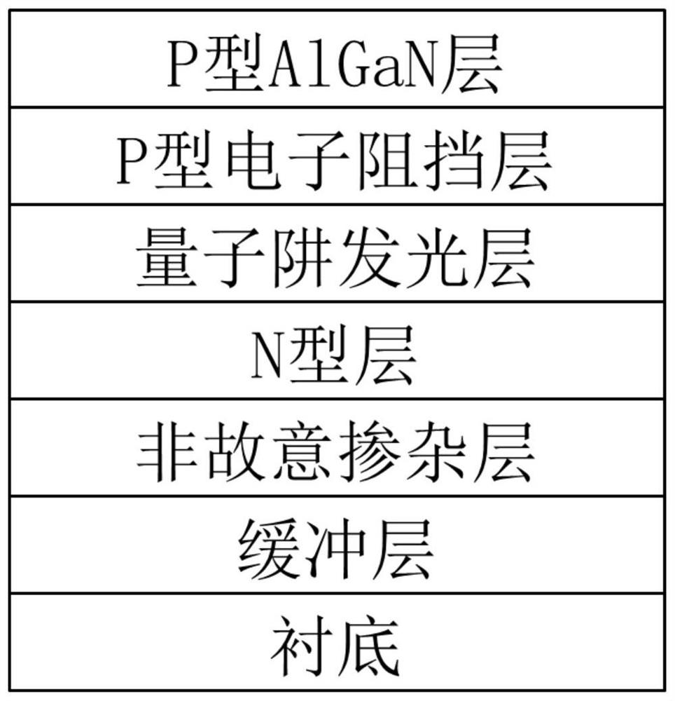
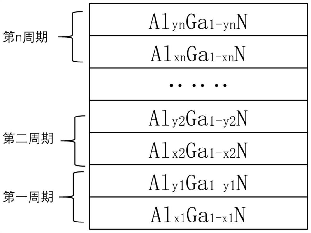
[0040] An ultraviolet LED epitaxial structure, including a substrate, a buffer layer, an unintentionally doped layer, an N-type layer, a quantum well light-emitting layer, a P-type electron blocking layer, and a P-type AlGaN layer arranged from bottom to top; the quantum well emits light layer is Al with multiple periods x Ga 1- x N / Al y Ga 1-y N superlattice structure, the Al x Ga 1-x N / Al y Ga 1-y N superlattice structure including Al x Ga 1-x N well layer and Al y Ga 1-y N barrier layer;
[0041] The period number n of the superlattice structure is 5: the first periodic structure is Al x1 Ga 1-x1 N / Al y1 Ga 1-y1 N; the second periodic structure is Al x2 Ga 1-x2 N / Al y2 Ga 1-y2 N; the third periodic structure is Al x3 Ga 1-x3 N / Al y3 Ga 1-y3 N; the third periodic structure is Al x3 Ga 1- x3 N / Al y3 Ga 1-y3 N; the fourth periodic structure is Al x4 Ga 1-x4 N / Al y4 Ga 1-y4 N; the fifth periodic structure is Al x5 Ga 1-x5 N / Al y5 Ga 1-y5 N. ...
Embodiment 2
[0051] An ultraviolet LED epitaxial structure, including a substrate, a buffer layer, an unintentionally doped layer, an N-type layer, a quantum well light-emitting layer, a P-type electron blocking layer, and a P-type AlGaN layer arranged from bottom to top; the quantum well emits light layer is Al with multiple periods x Ga 1- x N / Al y Ga 1-y N superlattice structure, the Al x Ga 1-x N / Al y Ga 1-y N superlattice structure including Al x Ga 1-x N well layer and Al y Ga 1-y N barrier layer;
[0052] The period number n of the superlattice structure is 6: the first periodic structure is Al x1 Ga 1-x1 N / Al y1 Ga 1-y1 N; the second periodic structure is Al x2 Ga 1-x2 N / Al y2 Ga 1-y2 N; the third periodic structure is Al x3 Ga 1-x3 N / Al y3 Ga 1-y3 N; the third periodic structure is Al x3 Ga 1- x3 N / Al y3 Ga 1-y3 N; the fourth periodic structure is Al x4 Ga 1-x4 N / Al y4 Ga 1-y4 N; the fifth periodic structure is Al x5 Ga 1-x5 N / Al y5 Ga 1-y5 N; t...
PUM
| Property | Measurement | Unit |
|---|---|---|
| thickness | aaaaa | aaaaa |
| thickness | aaaaa | aaaaa |
| thickness | aaaaa | aaaaa |
Abstract
Description
Claims
Application Information


