Parallel electron beam detection system based on nanometer electron source

A detection system and electron source technology, which is applied in the direction of material analysis, measuring devices, and instruments using wave/particle radiation, can solve problems such as low detection efficiency, damage to inspected materials, inspected devices, and increased electronic Coulomb force. Achieve high electron emission rate, improve efficiency, and small curvature radius

Pending Publication Date: 2021-12-10
XI'AN INST OF OPTICS & FINE MECHANICS - CHINESE ACAD OF SCI
View PDF8 Cites 0 Cited by
  • Summary
  • Abstract
  • Description
  • Claims
  • Application Information

AI Technical Summary

Problems solved by technology

For a long time, electron beam detection has technical bottlenecks such as a small number of electron beams and low detection efficiency, which greatly reduces the detection speed of the inspected materials and devices.
For many years, scientific researchers have been working on the research of high-efficiency electron beam detection systems. By increasing the energy and current of the electron beam, the detection efficiency of the electron beam can be improved to a certain extent, but at the same time, due to the high energy of the electrons and the excessive beam current The material under test, the device under test causes damage, or the detection resolution is reduced due to the increase of electron Coulomb force

Method used


Image

  • Parallel electron beam detection system based on nanometer electron source
  • Parallel electron beam detection system based on nanometer electron source

Examples


Embodiment 1

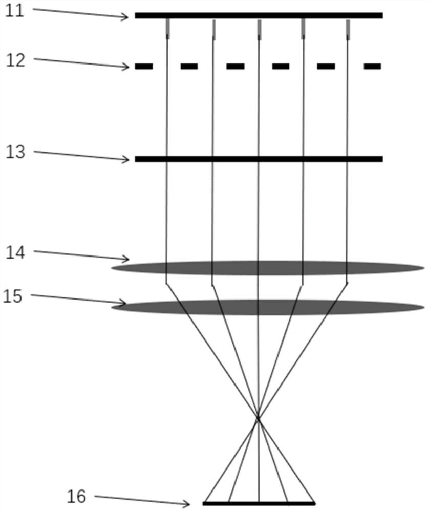
[0017] Such as figure 1 As shown, the parallel electron beam detection system based on the nano-electron source of the present invention includes a nano-array electron source 11, an accelerating electrode array 12, a sample stage 13, an objective lens 14, a correcting mirror 15, a detector 16, and the like arranged in sequence. The nano-array electron source 11 emits multiple beams of electrons under the pull of the accelerating electrode based on the field emission effect, the accelerating electrode array 12 accelerates the multiple beams of electrons emitted by the nano-array electron source 11 to a certain energy, and the sample stage 13 receives the multiple beams of electrons and makes the electrons penetrate In order to obtain the internal structure information of the sample, the objective lens 14 and the correcting mirror 15 form an electron optical system, which focuses the electrons passing through the sample and images them to the detector 16 at a fixed zoom ratio.

...

Embodiment 2

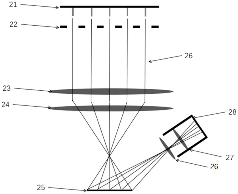
[0021] The electron beam detection system of the present invention is not limited to the transmission imaging system, and can also be applied to the electron beam detection system based on the secondary electron emission system. The electrons emitted by the nano-array electron source 21 are bombarded to be tested after passing through the accelerating pole and focusing by the electron optical system. The surface of the device 25 , the secondary electrons emitted from the surface 25 of the device to be tested are collected by the electron optical system and imaged at the detector 28 .

[0022] Such as figure 2 As shown, the parallel electron beam detection system based on the nano-electron source of the present invention includes a nano-array electron source 21, an accelerating electrode array 22, a first electron optical unit, a second electron optical unit and a detector 28; the first electron optical unit includes The first objective lens 23, the first correcting mirror 24;...


PUM


Abstract

The invention provides a parallel electron beam detection system based on a nanometer electron source. The parallel electron beam detection system based on the nanometer electron source is efficient and high in precision, the electron beam detection efficiency can be improved, and the electron beam detection aberration can be improved. The parallel electron beam detection system based on the nanometer electron source comprises a nanometer array electron source, an accelerating electrode array, a sample table, an objective lens, a correction lens and a detector which are arranged in sequence; the nanometer array electron source emits multiple beams of electrons based on a field emission effect, the accelerating electrode array accelerates the multiple beams of electrons emitted by the nanometer array electron source, and the sample table receives the multiple beams of electrons and enables the multiple beams of electrons to penetrate through a sample so as to obtain internal structure information of the sample; and the multiple transmission electron beams are focused through the objective lens and the correction lens, aberration is corrected, and then a sample information image is presented on the detector.

Description

technical field [0001] The invention relates to the field of electron beam imaging detection, in particular to a parallel electron beam detection system based on a nanometer electron source. Background technique [0002] Electron beam detection has a very broad application prospect in the field of material device characterization. For a long time, electron beam detection has technical bottlenecks such as a small number of electron beams and low detection efficiency, which greatly reduces the detection speed of inspected materials and devices. For many years, scientific researchers have been working on the research of high-efficiency electron beam detection systems. By increasing the energy and current of the electron beam, the detection efficiency of the electron beam can be improved to a certain extent, but at the same time, due to the high energy of the electrons and the excessive beam current The material under test, the device under test cause damage, or the detection r...

Claims


Application Information

Patent Timeline
Patent Type & Authority Applications(China)
IPC IPC(8): G01N23/2251
CPCG01N23/2251
Inventor 强鹏飞盛立志张雪晗杨向辉闫永清刘哲李林森周晓红赵宝升
Owner XI'AN INST OF OPTICS & FINE MECHANICS - CHINESE ACAD OF SCI
Why Eureka
Try Eureka