Electronic emitting element, electronic source, image displaying device, and their mfg. method

A technology of electron emission and manufacturing method, which is applied in the manufacture of discharge tubes/lamps, electrical components, electrode systems, etc. It can solve the problems of uniformity reduction, complicated process management, and difficulty in forming film thickness with high precision.

Inactive Publication Date: 2003-12-24
CANON KK
View PDF8 Cites 0 Cited by
  • Summary
  • Abstract
  • Description
  • Claims
  • Application Information

AI Technical Summary

Problems solved by technology

[0021] 1) In the case of using a conductive film, it is difficult to form the film thickness and film material with high precision, and it becomes the main cause of the decrease in uniformity in the case of forming a plurality of electron emission elements such as a flat display panel
[0022] 2) In order to form a narrow gap with good electron emission characteristics, there must be a process of forming a gas atmosphere containing organic substances, and a process of forming a high-precision polymer on a conductive film. There are many additional processes and process management is also difficult. complicated
[0029] In the "molding process" and "activation process", there are many additional steps such as repeated energization steps and the step of forming an appropriate gas atmosphere in each step, and the management of each step is complicated.

Method used


Image

  • Electronic emitting element, electronic source, image displaying device, and their mfg. method
  • Electronic emitting element, electronic source, image displaying device, and their mfg. method
  • Electronic emitting element, electronic source, image displaying device, and their mfg. method

Examples


Embodiment 1

[0335] This example is an example of manufacturing the electron-emitting element of the present invention shown in FIG. 1 .

[0336] Since the following laser beams can pass through the substrate by using a glass substrate as the substrate 1 , laser irradiation can be performed regardless of the front and back of the glass substrate. As a material of the opposing electrodes 2 and 3, platinum which has high heat resistance against the following laser irradiation and especially high thermal conductivity is used. As the polymer film 4, aromatic polyimide is used.

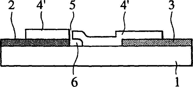
[0337] Hereinafter, the method of manufacturing the electron emission element of this embodiment will be described using FIG. 1, FIG. 2, and FIG. 3. FIG.

[0338] (Process 1)

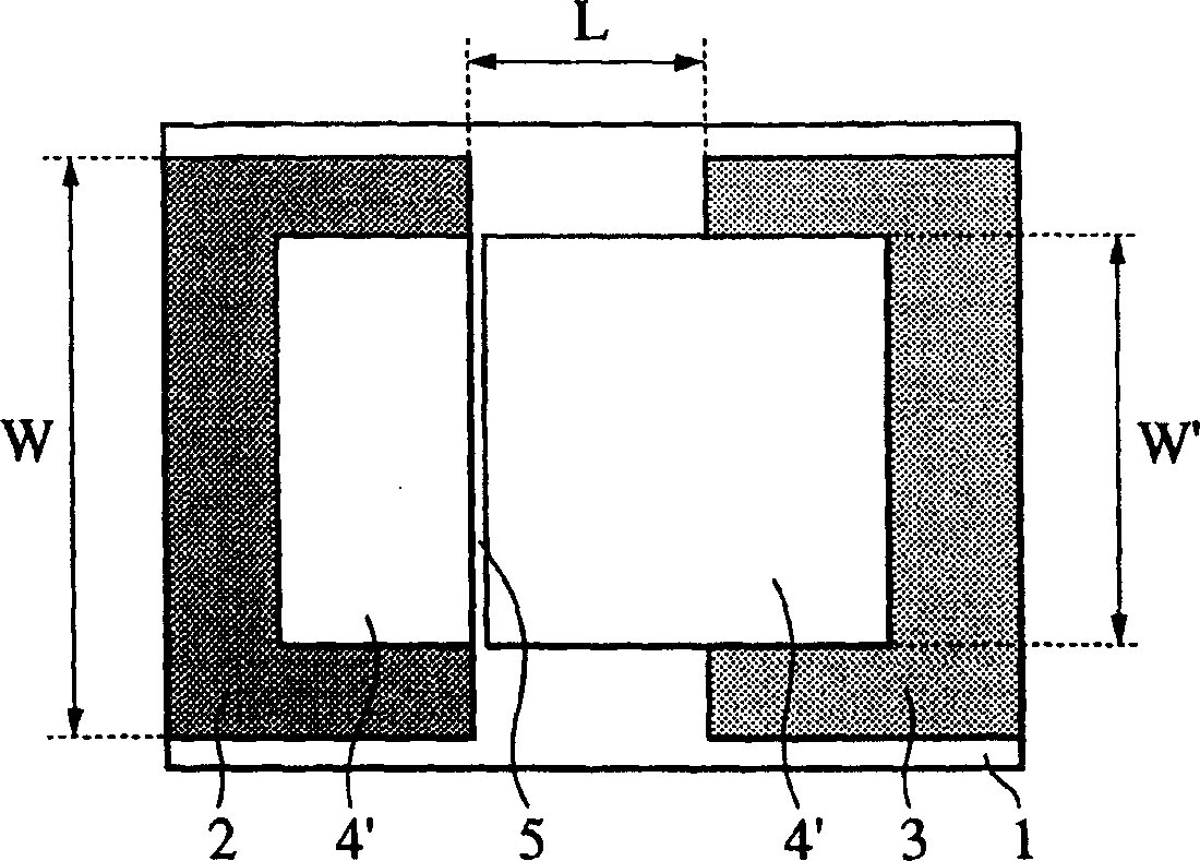
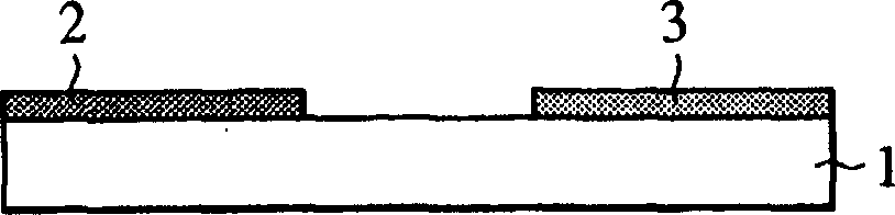
[0339] Use quartz glass as the substrate 1, clean the substrate 1 sufficiently with detergent, pure water, organic solvent, etc. Electrodes 2, 3 are formed thereon (FIG. 2(a)). At this time, the electrode interval L was set to 10 μm, the wid...

Embodiment 2

[0355] In this example, basically, an electron emission element was produced by the same process as in Example 1, but in this example, electron beam irradiation was used for the low-resistance treatment. Therefore, here, the steps after the step 3 of the first embodiment will be described using FIG. 8 .

[0356] (Process 3)

[0357] Place the substrate 1 formed with the electrodes 2, 3 and the polymer film 4 in a vacuum container equipped with an electron gun. After sufficient exhaust, the irradiation position of the center of the electron beam comes to the electrode 3, and on the electrode 3 Electron beams are irradiated (see Fig. 8(a), (b)). The irradiation condition of the electron beam at this time was set so that the accelerating voltage Vac=10 kV. The spot diameter of the electron beam is set at about 200 μm, and the center thereof is set at a distance of 100 μm or more upward from the end of the electrode 3, and the electron beam is directly irradiated between the ele...

Embodiment 3

[0367] The electron emission element of this embodiment is basically the same form as the electron emission element of the above-mentioned embodiment, but the manufacturing method is partially different.

[0368] First, electrodes 2 and 3 and a polymer film 4 made of a polyimide film were fabricated on a substrate 1 made of quartz glass in the same manner as Steps 1 and 2 of Example 1. The electrode interval L was wider than the previous embodiment and was set to 20 µm, the width W of the electrodes was set to 500 µm, and the thickness thereof was set to 100 nm. In addition, the width W' of the polymer film 4 was set to 300 µm.

[0369] When the electrode interval L is wide, as shown in Example 1 or Example 2, in the process of reducing the resistance of the polymer film 4 caused by electrode heating and heat conduction, the electrical resistance of the polymer film 4 cannot be sufficiently changed. The case of conduction characteristics.

[0370] Therefore, the process of u...


PUM


Abstract

The present invention provides an electron emitting device including electrodes (2,3) disposed with a space therebetween on a surface of a substrate (1), a carbon film (4') disposed between the electrodes and connected to one of the electrodes, and a gap (5) disposed between the carbon film and the other electrode. In the gap, the distance between the edge of the carbon film connected to one of the electrode and the edge of the other electrode at an upper position apart from the surface of the substrate is smaller than that at the surface of the substrate. The present invention also provides an electron source and an image display device each including the electron emitting device.

Description

technical field [0001] The present invention relates to electron emission elements, electron sources, image display devices, and their manufacturing methods. Background technique [0002] Conventionally, two types of electron emission elements using a hot cathode electron emission element and a cold cathode electron emission element are generally known. Among cold cathode electron emission elements, there are electric field emission type (hereinafter referred to as "FE type"), metal / insulator / metal type (hereinafter referred to as "MIM" type), and surface conduction type electron emission elements. [0003] As examples of FE type, there are in W.P.Dyke & W.W.Dolan, "Fieldemission", Advance in Electroron Physics, 8, 89 (1956) or C.A.Spindt, "PHYSICAL Properties of thin-film field emission cathodes with molybdenium cones", J.Appl Examples disclosed in .Phys., 47, 5248 (1976), JP-A-3-46729 and the like. [0004] As an example of the MIM type, there is an example disclosed in ...

Claims


Application Information

Patent Timeline
Patent Type & Authority Applications(China)
IPC IPC(8): H01J1/316H01J9/02H01J29/04H01J31/12
CPCH01J1/316H01J9/027H01J1/30
Inventor 教学正文水野祐信浜元康弘宫崎和也
Owner CANON KK
Why Eureka
Try Eureka