Cathode material used for PETE device

A cathode material and device technology, which is applied in the direction of electrical components, chemical instruments and methods, and parts of discharge tubes/lamps, etc., can solve the problems of low electron emission rate and weak sunlight absorption ability, so as to improve electron emission rate, Facilitates absorption and increases the effect of scattering centers

Inactive Publication Date: 2017-04-19
CHINA ELECTRONIC TECH GRP CORP NO 18 RES INST
View PDF5 Cites 0 Cited by
  • Summary
  • Abstract
  • Description
  • Claims
  • Application Information

AI Technical Summary

Problems solved by technology

[0004] At present, the published technical literature reports that most of the cathode materials used in current PETE device research are homogeneous P-type semiconductor materials, which have technical problems such as low electron emission rate and weak sunlight absorption ability.

Method used


Image

  • Cathode material used for PETE device

Examples


Embodiment 1

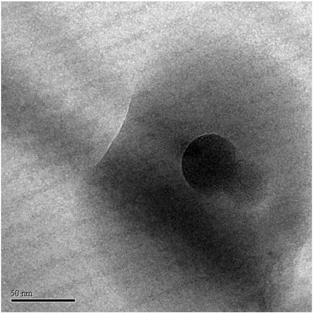
[0018] A kind of cathode material for PETE device, prepares Si 90 Ge 10 +0.05 mol% B sample. The cathode material for PETE devices selects silicon Si with a wide band gap and germanium Ge to form a binary solid solution compound material, and the compound is doped with element boron (B), and the molecular formula of the semiconductor compound formed is Si 90 Ge 10 +0.05 mol% B. Nanostructure formation method: adding boron nitride (BN) or carbon 60 (C 60 ) nanoparticles; the sintered material is cut into thin slices with a thickness of 2mm-5mm, and corroded in nitric acid with a concentration of 40%-80% at 80°C-120°C for 2min-5min. The material alloy is synthesized by intermediate frequency smelting, and the alloy is rapidly sintered by spark plasma sintering (SPS).

[0019] The cathode material for PETE devices has an electron work function of 4.32 eV at room temperature, which is lower than that of conventional B-doped Si materials (about 4.4 eV); the work function of sa...

Embodiment 2

[0021] A kind of cathode material for PETE device, prepares Si 90 Ge 10 Material samples with +0.05mol% B and 2vol% Al pore former added. The cathode material for PETE devices selects silicon Si with a wide band gap and germanium Ge to form a binary solid solution compound material, and the compound is doped with element boron (B), and the molecular formula of the semiconductor compound formed is Si 90 Ge 10 +0.05 mol% B. Nanostructure generation method: Add aluminum Al nanoparticles as a pore-forming agent in the alloy powder film, the addition ratio is 2vol%, and then cut the sintered material into thin slices with a thickness of 2mm-5mm, and place it at a concentration of 80°C-120°C It is corroded in 40%-80% nitric acid for 2min-5min; the material alloy is synthesized by intermediate frequency smelting, and the alloy is rapidly sintered by spark plasma sintering (SPS).

[0022] The cathode material for PETE devices has an electron work function of 4.08ev at room tempera...


PUM


Abstract

The invention relates to a cathode material used for a PETE device and belongs to the technical field of photoelectric thermoelectric power generation. The cathode material used for the PETE device is a binary solid solution compound formed by silicon and germanium, and the molecular formula of the semiconductor compound is Si<x>Ge<1-X>, wherein x equals 5-30%; the compound is doped with an element boron (B), and the doping proportion is 0.02-0.08mol%; a nanostructure is generated in two manners: one manner is that boron nitride (BN) or carbon 60 (C60) nanoparticles are added to alloy powder, and the adding weight proportion is 0.2-0.5wt%; the other manner is that aluminum nanoparticles are added to the alloy powder to serves as a pore-forming agent, the adding proportion is 1-5vol%, then a sintered material is sliced into thin sheets which are 2-5 mm in thickness, and the sheets are placed in nitric acid at the temperature of 80-120 DEG C with the mass concentration being 40%-80% to be corroded. By means of the cathode material, the scattering center of the material can be effectively increased, the electron emissivity of the cathode material can be remarkably improved, it is beneficial for the cathode to absorb sunlight, the effect is obvious, and the application range is wide.

Description

technical field [0001] The invention belongs to the technical field of photoelectric thermoelectric power generation, and in particular relates to a cathode material for PETE devices. Background technique [0002] PETE devices are also called photon-enhanced thermionic emission devices, which can use light and heat to generate electricity at the same time. very few). The structure of the device is similar to that of the thermionic emission device, both of which are vacuum flat plates with two electrodes, the cathode and the anode, and the difference is that the cathode is a P-type semiconductor. The power generation principle of this device is: the cathode absorbs photons, and the electrons transition from the valence band to the conduction band through thermal excitation; the electrons diffuse to the cathode surface, overcome the potential barrier and emit into the vacuum; the anode collects charges to form a current. [0003] According to the working principle of the PET...

Claims


Application Information

Patent Timeline
Patent Type & Authority Applications(China)
IPC IPC(8): C01G17/00H01J1/308
CPCC01G17/006C01P2004/03C01P2004/80H01J1/308
Inventor 张丽丽任保国
Owner CHINA ELECTRONIC TECH GRP CORP NO 18 RES INST
Why Eureka
Try Eureka