Three-dimensional integrated chip

A three-dimensional integration and chip technology, applied in the fields of instruments, electrical digital data processing, electrical components, etc., can solve the problems of limited storage access bandwidth, insufficiency of storage capacity, etc., to solve the problem of storage walls, high bandwidth, and low power consumption. Effect

Pending Publication Date: 2021-12-14
XI AN UNIIC SEMICON CO LTD
View PDF0 Cites 0 Cited by
  • Summary
  • Abstract
  • Description
  • Claims
  • Application Information

AI Technical Summary

Problems solved by technology

The storage access capacity and bandwidth of the reconfigurable unit are greatly increased, and the storage capacity of the static storage array in the FPGA / eFPGA component is usually unable to meet, and then turn to the storage access outside the FPGA / eFPGA component, and the interconnection bit of the storage access outside the FPGA / eFPGA component The width and distance are obviously inferior to the connection in FPGA / eFPGA components, which limits the storage access bandwidth, and the power consumption overhead is much higher than that in FPGA / eFPGA components, forming a storage wall

Method used


Image

  • Three-dimensional integrated chip
  • Three-dimensional integrated chip
  • Three-dimensional integrated chip

Examples


Embodiment Construction

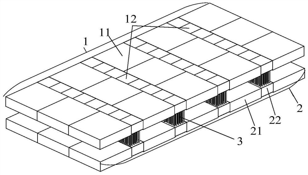
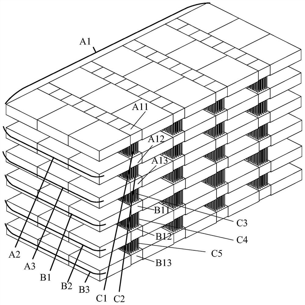
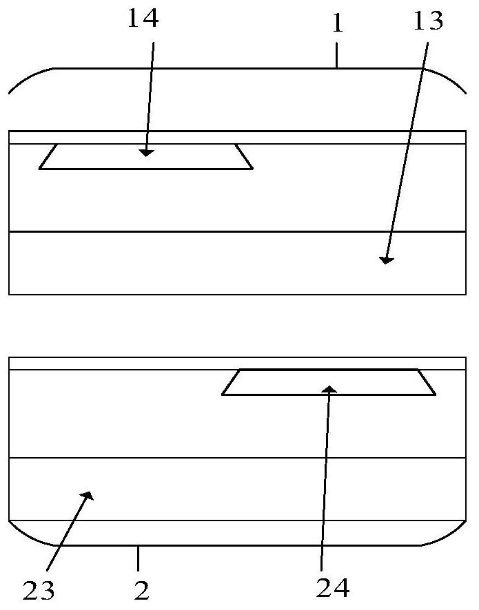
[0036] In this application, the above-mentioned components may be at least one of a die or chip and a wafer, but it is not limited thereto, and it may also be any replacement conceivable by those skilled in the art. .

[0037] Wherein, a wafer refers to a silicon wafer used for manufacturing a silicon semiconductor circuit, and a chip or a die refers to a silicon wafer obtained by dividing the above-mentioned wafer on which a semiconductor circuit is manufactured. In the specific embodiments of the present application, crystal grains are taken as an example for introduction. For example: the programmable array component is a programmable array die.

[0038]With the large-scale growth of data processing requirements, the reconfigurable architecture based on traditional FPGA / eFPGA faces the challenge of storage access. The storage access capacity and bandwidth of the reconfigurable unit are greatly increased, and the storage capacity of the static storage array in the FPGA / eFP...


PUM


Abstract

The invention provides a three-dimensional integrated chip. The chip comprises: a first programmable array assembly which comprises a first bonding region; a first storage array assembly which comprises a second bonding region; and a second storage array assembly which comprises a third bonding region. The first bonding region is in bonding connection with the second bonding region, and the second bonding region is in bonding connection with the third bonding region, so that the first programmable array assembly, the first storage array assembly and the second storage array assembly are bonded. Therefore, the storage space of the first programmable array assembly is expanded, the first programmable array assembly, the first storage array assembly and the second storage array assembly are bonded through the three-dimensional bonding technology, the interconnection distance is reduced, high bandwidth and low power consumption of storage access are achieved, and the storage wall problem existing in the prior art is solved.

Description

technical field [0001] The invention relates to the technical field of integrated circuits, in particular to a three-dimensional integrated chip. Background technique [0002] With the large-scale growth of data processing requirements, the reconfigurable architecture based on traditional FPGA / eFPGA faces the challenge of storage access. The storage access capacity and bandwidth of the reconfigurable unit are greatly increased, and the storage capacity of the static storage array in the FPGA / eFPGA component is usually not enough, and then it turns to the storage access outside the FPGA / eFPGA component, and the interconnection bit of the storage access outside the FPGA / eFPGA component The width and distance are obviously inferior to the connection in FPGA / eFPGA components, which limits the storage access bandwidth, and the power consumption overhead is much higher than that in FPGA / eFPGA components, forming a storage wall. Contents of the invention [0003] The invention p...

Claims


Application Information

Patent Timeline
Patent Type & Authority Applications(China)
IPC IPC(8): H01L25/065G06F15/78
CPCH01L25/0657G06F15/7839Y02D10/00
Inventor 任奇伟左丰国周骏郭一欣江喜平
Owner XI AN UNIIC SEMICON CO LTD
Why Eureka
Try Eureka