A vertical interconnect substrate based on laser nanoprocessing technology and its manufacturing method

A nano-fabrication and vertical interconnection technology, which is applied in the manufacture of printed circuits, mechanically removing conductive materials, and electrically connecting printed components, can solve problems such as large parasitic inductance and capacitance, low system integration, and long signal delays. problem, achieve the effect of reducing parasitic inductance and capacitance, simplifying the process, and reducing signal delay

Active Publication Date: 2022-01-25
SHANGHAI SPACEFLIGHT ELECTRONICS & COMM EQUIP RES INST
View PDF17 Cites 0 Cited by
  • Summary
  • Abstract
  • Description
  • Claims
  • Application Information

AI Technical Summary

Problems solved by technology

However, the traditional pure PTFE material has low strength and must be filled with reinforcing materials such as glass fibers before it can be used as a substrate.
[0004] As a new type of microwave / millimeter-wave substrate material, LCP can not only meet the requirements of high-performance microwave / millimeter-wave systems, but also microwave devices based on LCP can be used in bending or even folding environments, so it has received extensive attention in system integration application research. , but the existing LCP substrates for electronic packaging still have the disadvantages of long signal delay, large parasitic inductance and capacitance, and low system integration

Method used


Image

  • A vertical interconnect substrate based on laser nanoprocessing technology and its manufacturing method
  • A vertical interconnect substrate based on laser nanoprocessing technology and its manufacturing method
  • A vertical interconnect substrate based on laser nanoprocessing technology and its manufacturing method

Examples


Embodiment 1

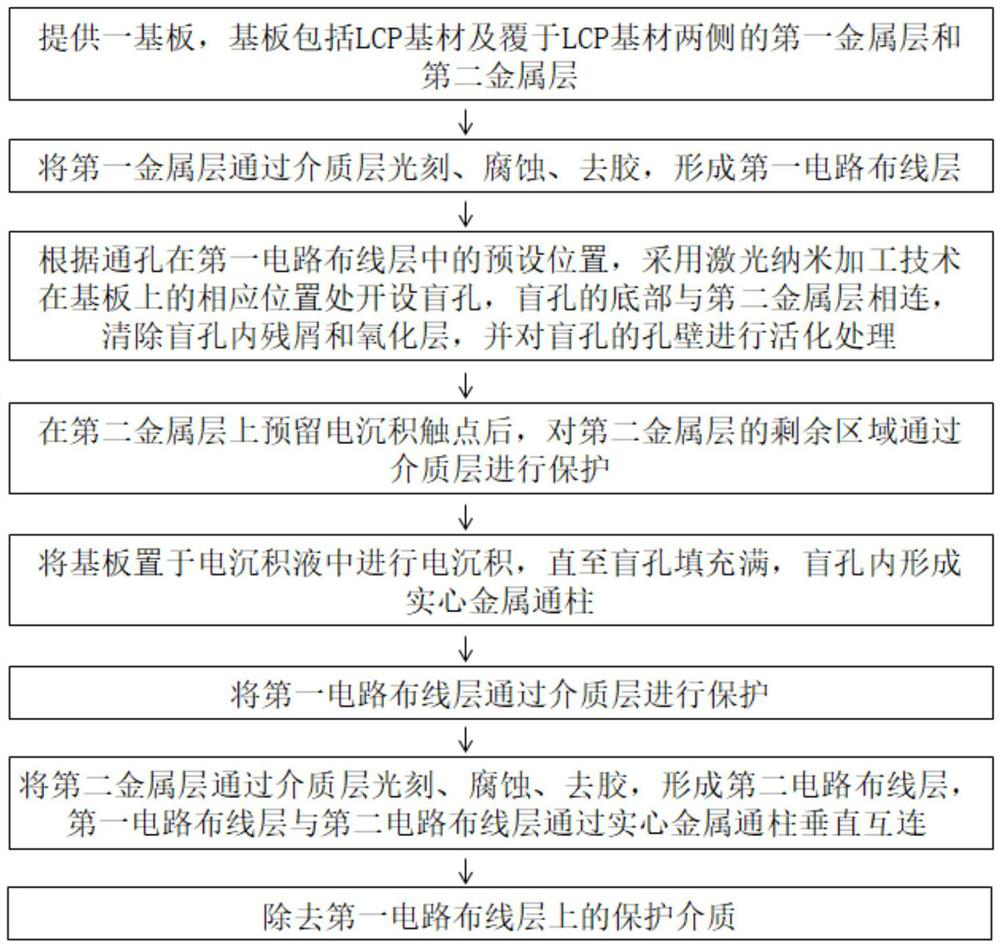
[0046] see figure 1 and Figures 2a to 2d as shown, figure 1 It is a flowchart of a method for manufacturing a vertically interconnected substrate based on laser nanoprocessing technology according to an embodiment of the present invention. The present invention provides a method for manufacturing a vertically interconnected substrate based on laser nanoprocessing technology, including the following steps:

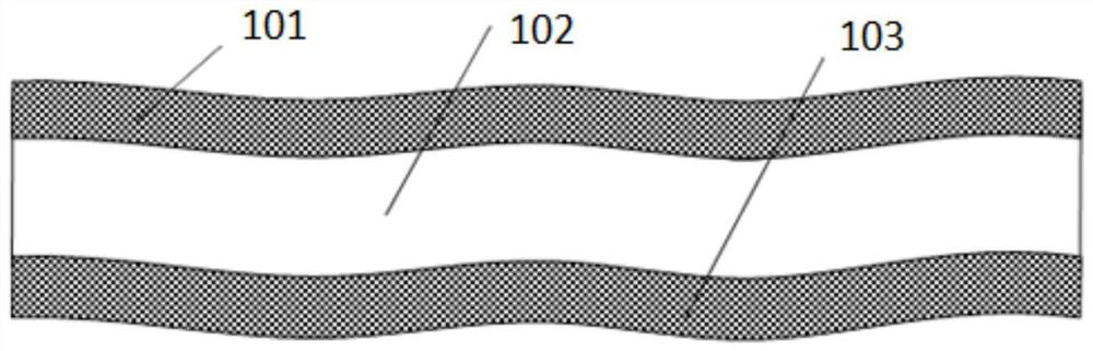
[0047] S1: provide a substrate, see Figure 2a As shown, the substrate includes an LCP substrate 102 and a first metal layer 101 and a second metal layer 103 covering both sides of the LCP substrate 102. In this embodiment, the first metal layer 101 and the second metal layer 103 are both copper layer;

[0048] S2: see Figure 2b As shown, the first metal layer 101 is formed through positive photoresist photolithography, hard film, excess copper corrosion, and glue removal to form the first circuit wiring layer 105;

[0049] S3: see Figure 2b As shown, according to ...

Embodiment 2

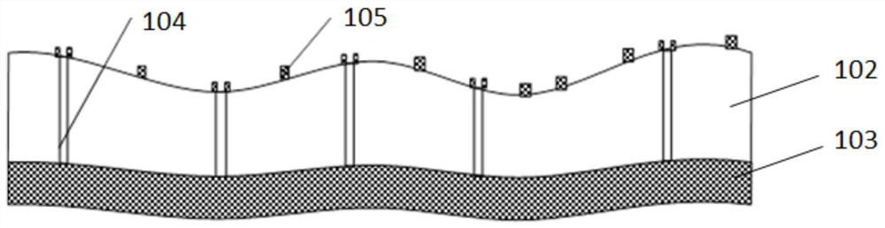
[0060] Based on the same inventive concept, such as Figure 2d As shown, the present invention also provides a vertical interconnect substrate based on laser nanoprocessing technology, which is manufactured by the vertical interconnect substrate manufacturing method based on laser nanoprocessing technology described in Embodiment 1, which includes At least one solid metal via 106, the first circuit wiring layer 105, the LCP substrate 102 and the second circuit wiring layer 107, the first circuit wiring layer 105 and the second circuit wiring layer 107 are respectively covered on both sides of the LCP substrate 102, The solid metal via 106 is a metal conductor for vertically interconnecting the first circuit wiring layer 105 and the second circuit wiring layer 107 in the substrate. Preferably, the materials of the first circuit wiring layer 105, the second circuit wiring layer 107 and the solid metal via post 106 are all copper, and metallized through holes are used to realize ...

Embodiment 3

[0064] Based on the same inventive concept, such as Figure 5 as shown, Figure 5 It is a flowchart of a method for manufacturing a vertically interconnected substrate based on laser nanoprocessing technology according to an embodiment of the present invention. The present invention also provides a method for manufacturing a vertically interconnected substrate based on laser nanoprocessing technology, including the following steps:

[0065] S1: provide a substrate, the substrate includes an LCP substrate and a first metal layer and a second metal layer covering both sides of the LCP substrate;

[0066] S2: According to the preset position of the through hole in the first metal layer, laser nanoprocessing technology is used to open a blind hole at the corresponding position on the substrate, and the bottom of the blind hole is connected to the second metal layer, and the blind hole is cleaned. ;

[0067] S3: after reserving electrodeposited contacts on the second metal layer,...


PUM

PropertyMeasurementUnit
thicknessaaaaaaaaaa
wavelengthaaaaaaaaaa
thicknessaaaaaaaaaa

Abstract

The invention discloses a method for manufacturing vertically interconnected substrates based on laser nano-processing technology. Firstly, a first circuit wiring layer is formed on one side of the substrate through photolithography, corrosion, and glue removal of the dielectric layer, and then the laser nano-processing technology is used to form the first circuit wiring layer on one side of the substrate. Blind holes are opened at the corresponding positions on the substrate, and then the substrate is placed in the electrodeposition solution for electrodeposition to fill the blind holes, and finally the second circuit is formed on the other side of the substrate through photolithography, corrosion, and degumming of the dielectric layer Wiring layer, the manufacturing method has a simple process, high precision of laser nano-processing technology, no void inside the through hole, reliable interconnection, and improves the density and reliability of the three-dimensional packaging of the LCP flexible substrate. At the same time, the metallized through hole is used to realize the double The vertical interconnection between the surface circuit wiring layers can effectively shorten the interconnection distance, reduce signal delay, reduce parasitic inductance and capacitance, improve high-frequency characteristics, and thus improve system integration performance.

Description

technical field [0001] The invention belongs to the technical field of electronic packaging, and in particular relates to a vertical interconnect substrate based on laser nano-processing technology and a manufacturing method thereof. Background technique [0002] With the development of electronic products in the direction of thinner, lighter, wearable and multifunctional, higher requirements are put forward for packaging substrates in terms of miniaturization, flexibility and high density. At present, the flexible substrate materials used for microwave / millimeter wave mainly include: polyimide (PI), polyethylene (PE), thermoplastic polymer (PEN, PET) and liquid crystal polymer (Liquid Crystal Polymer, LCP) and so on. Compared with other flexible materials, LCP has high molecular structure symmetry and weak dipole polarization, making it a high-performance flexible substrate material. [0003] LCP materials can maintain low dielectric constant and tangent loss in a very wid...

Claims


Application Information

Patent Timeline
Patent Type & Authority Patents(China)
IPC IPC(8): H05K1/02H05K1/09H05K1/11H05K3/00H05K3/04H05K3/10H05K3/18H05K3/42
CPCH05K3/42H05K3/00H05K3/046H05K3/107H05K3/18H05K3/188H05K1/02H05K1/09H05K1/116
Inventor 刘凯张诚丁蕾罗燕任卫朋王立春
Owner SHANGHAI SPACEFLIGHT ELECTRONICS & COMM EQUIP RES INST
Why Eureka
Try Eureka