Micro-damage cutting system and method for photovoltaic crystalline silicon solar cell

A solar cell, photovoltaic crystalline silicon technology, applied in photovoltaic power generation, circuits, electrical components, etc., can solve problems such as reducing production safety, affecting cell strength, reducing conversion efficiency, etc., and reducing heat-affected areas and cross-section microcracks , Avoid the risk of cracking, improve the effect of product strength

Pending Publication Date:
View PDF9 Cites 0 Cited by
  • Summary
  • Abstract
  • Description
  • Claims
  • Application Information

AI Technical Summary

Problems solved by technology

The disadvantages of this processing method are: 1. During the process of laser material removal, a large amount of dust will be formed, which is harmful to human health, and it is easy to cause equipment fires, seriously reducing production safety; 2. While laser material removal, cutting There will also be a large number of microcracks in the area, which will affect the strength of the cut cell and reduce the service life of the photovoltaic module after packaging. On the other hand, defects will be formed inside the crystalline silicon to reduce the conversion efficiency of the cell; 3. High peak power The interaction between the pulsed laser and the material causes the temperature to rise rapidly and spread to the surrounding area, forming a certain range of heat-affected areas at the cutting edge, destroying the surface structure of the cell and reducing the conversion efficiency; 4. After the pulsed laser removes the material, it is necessary to use mechanical breaking In the process, it is easy to cause damage and cracks of the cell

Method used


Image

  • Micro-damage cutting system and method for photovoltaic crystalline silicon solar cell
  • Micro-damage cutting system and method for photovoltaic crystalline silicon solar cell
  • Micro-damage cutting system and method for photovoltaic crystalline silicon solar cell

Examples


Embodiment

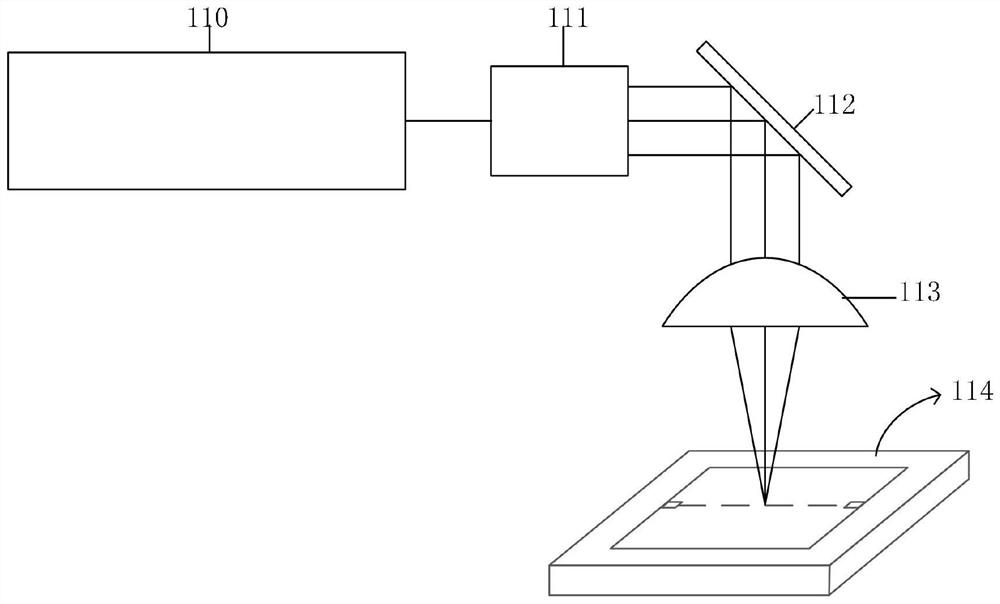
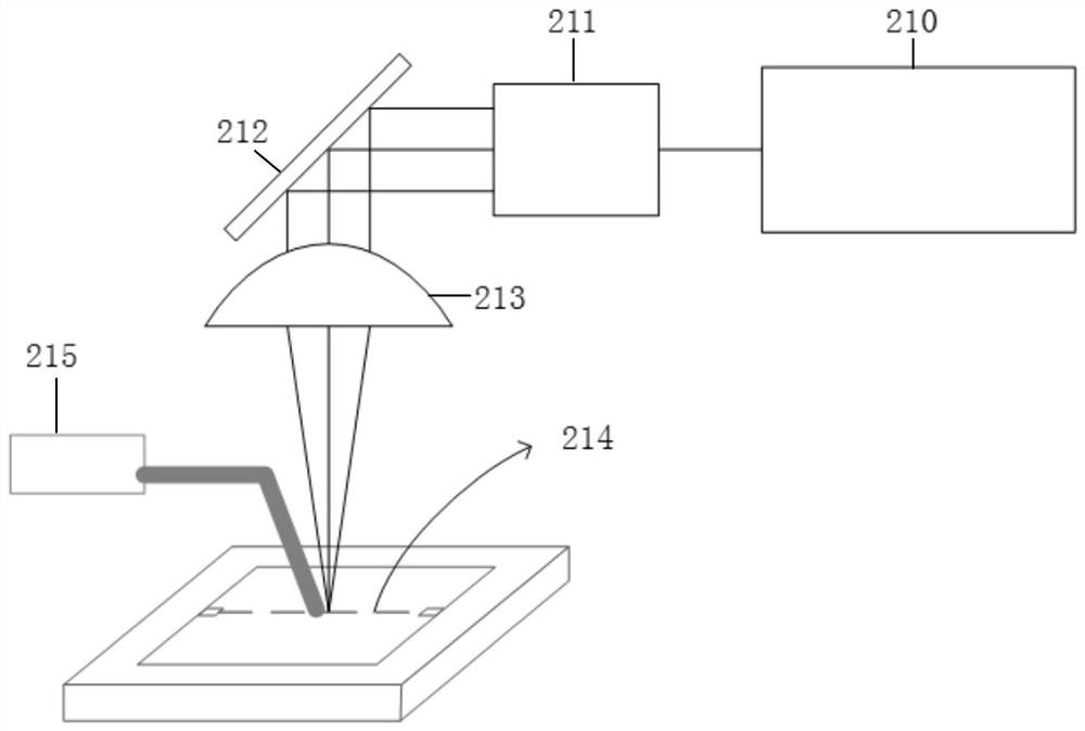
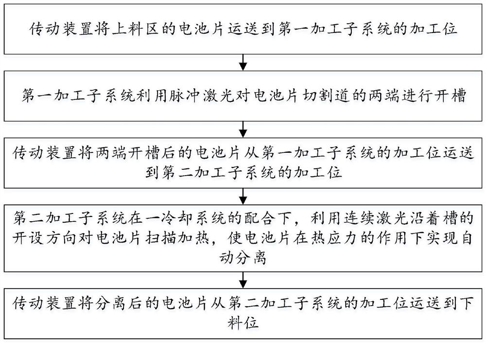
[0046] A micro-damage cutting system for photovoltaic crystalline silicon solar cells, such as Figure 1 to Figure 10 As shown, the micro-damage cutting system for photovoltaic crystalline silicon solar cells includes a first processing subsystem, a second processing subsystem and a transmission device; slotting, the second processing subsystem is used to scan and heat the cells along the opening direction of the slots with a continuous laser with the cooperation of a cooling system 215, so that the cells can be automatically separated under the action of thermal stress , the transmission device is used to transport the battery slices at the loading level to the processing position of the first processing subsystem, or transport the battery slices with both ends slotted from the processing position of the first processing subsystem to the The processing station of the second processing subsystem, or transport the separated battery slices from the processing station of the seco...


PUM

PropertyMeasurementUnit
wavelengthaaaaaaaaaa

Abstract

The embodiment of the invention belongs to the technical field of photovoltaic crystalline silicon solar cell cutting, and relates to a micro-damage cutting system and method for a photovoltaic crystalline silicon solar cell. The micro-damage cutting system for the photovoltaic crystalline silicon solar cell comprises a first processing subsystem, a second processing subsystem and a transmission device, the first processing subsystem is used for grooving the two ends of a cell cutting channel through pulse laser, and the second processing subsystem is used for scanning and heating cells in the grooving direction through continuous laser under the cooperation of a cooling system, so that the cells are automatically separated under the action of thermal stress. According to the micro-damage cutting system and method for the photovoltaic crystalline silicon solar cell, the micro-damage cutting system for the photovoltaic crystalline silicon solar cell can reduce heat affected areas and fracture surface microcracks in the cutting process of solar cells, improves product strength, avoids hidden crack risks, greatly reduces dust generated in the cutting process, and can be widely applied to the field of photovoltaic crystalline silicon solar cell cutting.

Description

technical field [0001] The present application relates to cutting technology for photovoltaic crystalline silicon solar cells, and more specifically, to a micro-damage cutting system and method for photovoltaic crystalline silicon solar cells. Background technique [0002] With the development of science and technology, people's awareness of environmental protection is constantly increasing. As a clean and renewable energy source, solar energy has attracted widespread attention. Crystalline silicon solar cells based on semiconductor technology are the core components of photovoltaic power generation. The larger the size of the cell and the higher the efficiency of the cell, the greater the short-circuit current of the device, resulting in greater packaging loss from the cell to the module, and the heat loss of the module outdoors. The risk of spotting increases, so it is inevitable to cut the cell, and the cell is divided into small pieces and then packaged, which can obtain...

Claims


Application Information

Patent Timeline
Patent Type & Authority Applications(China)
IPC IPC(8): B23K26/38B23K26/70H01L31/18
CPCB23K26/38B23K26/702H01L31/1804H01L31/1876Y02E10/547Y02P70/50
Inventor 陈锐卢建刚赖林松颜传祥任莉娜李启文周志伟尹建刚高云峰
Why Eureka
Try Eureka