A real-time controllable wave absorber based on ferroelectric ferromagnetic composite film loading
A composite film and wave absorber technology, applied in the direction of electrical components, antennas, etc., can solve the problems of inability to control in real time, unfavorable application environment of microwave devices, etc., and achieve the effect of flexible control
- Summary
- Abstract
- Description
- Claims
- Application Information
AI Technical Summary
Problems solved by technology
Method used
Image
Examples
Embodiment 1
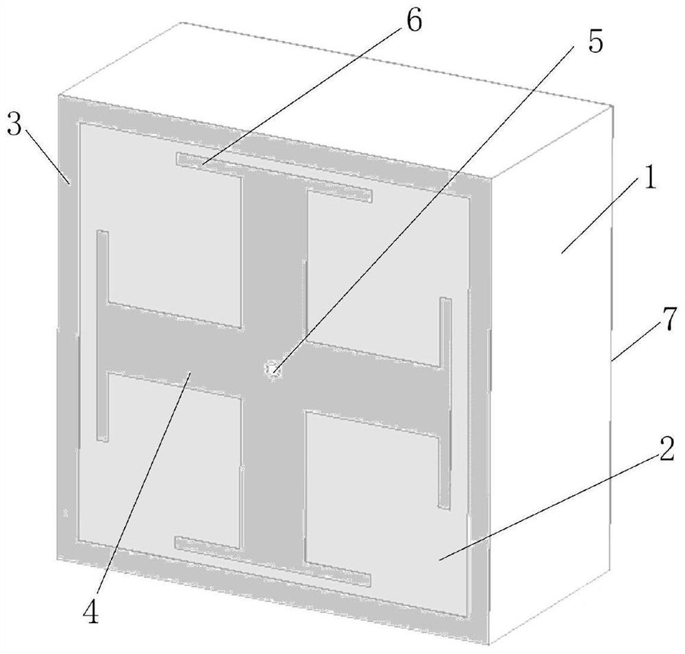
[0025] Example 1. A real-time controllable wave absorber based on ferroelectric ferromagnetic composite film loading, consisting of figure 1 As shown, including the dielectric plate 1, the front of the dielectric plate 1 is covered with a ferroelectric ferromagnetic composite film 2, the surface of the ferroelectric ferromagnetic composite film 2 is provided with a metal microstrip frame 3 along the edge of the dielectric plate 1, and the ferroelectric ferromagnetic composite film 2 is provided with a metal microstrip frame 3. 2. There is also a cross-shaped metal microstrip 4 in the center of the surface, and the middle of the cross-shaped metal microstrip 4 is connected to the metal layer 7 arranged on the back of the dielectric plate 1 through the metal via 5; The structure can adjust the wave absorption peak position of the wave absorber in real time by utilizing the characteristic that the dielectric constant and the magnetic permeability of the ferroelectric ferromagneti...
Embodiment 2
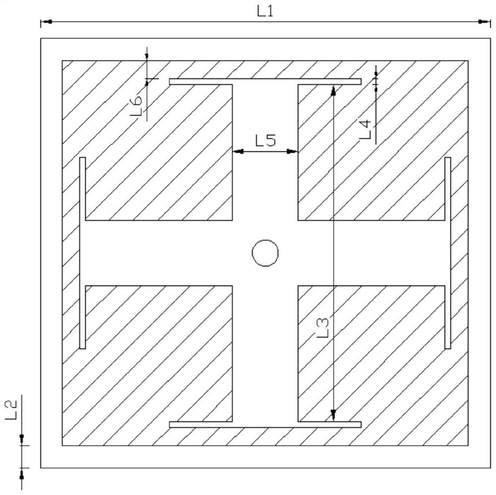
[0038] Example 2. A real-time controllable wave absorber based on ferroelectric ferromagnetic composite film loading, consisting of figure 1 and 2 The size parameters of each part are shown in Table 1.
[0039] Table 1
[0040] structure name symbol Dimensions (mm) Media board side length L 1
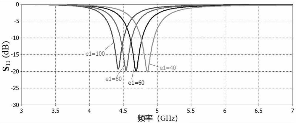
[0041] The dielectric plate of the absorber adopts BaAl with a dielectric constant of 5.0 2 Si 2 O 8 ceramic substrate, the absorber S 11 The calculation results of scattering parameters and electromagnetic field distribution using finite integration are as follows: Figures 3 to 6 shown. image 3 S is the absorber in the middle 11 The scattering characteristic diagram lists the absorption frequency diagram of the sample structure, and it can be seen that the structure has good absorption characteristics. Figure 3 to Figure 4 S after loading the bias electric field and magnetic field for the absorber 11 Reflection coefficient. The reflection characterist...
PUM
| Property | Measurement | Unit |
|---|---|---|
| thickness | aaaaa | aaaaa |
| thickness | aaaaa | aaaaa |
| relative permittivity | aaaaa | aaaaa |
Abstract
Description
Claims
Application Information


