Negative resistance clamping silicon controlled rectifier memory resistor device and manufacturing method thereof

A technology of memristive devices and silicon rectifiers, which is applied in the field of negative resistance clamped thyristor rectifier memristive devices and its production, can solve problems such as difficult integration of memristive devices, achieve good robustness, realize nonlinear characteristics, The effect of the simple production method

Pending Publication Date: 2021-12-24
HUNAN NORMAL UNIVERSITY
View PDF0 Cites 0 Cited by
  • Summary
  • Abstract
  • Description
  • Claims
  • Application Information

AI Technical Summary

Problems solved by technology

[0003] Nanoscale-based TiO 2 Solid-state thin-film two-terminal memristors such as figure 1 As shown, by constructing a boundary mobility model to explain the memristive phenomenon in the device, the device is equivalent to TiO with a thickness of D 2 , there is a highly doped region in the film, and the resistance value is expressed as R ON , a low doped region, the resistance value is denoted as R OFF , the total resistance of the device is equivalent to the sum of the series connection of two resistors, and the length of the high-concentration doped region is represented by the variable W. It is difficult to achieve large-scale on-chip integration with standard microelectronics processes for memristive devices realized by the above materials

Method used


Image

  • Negative resistance clamping silicon controlled rectifier memory resistor device and manufacturing method thereof
  • Negative resistance clamping silicon controlled rectifier memory resistor device and manufacturing method thereof
  • Negative resistance clamping silicon controlled rectifier memory resistor device and manufacturing method thereof

Examples


Embodiment Construction

[0028] The present invention will be described in further detail below in conjunction with the accompanying drawings and embodiments. It should be understood that the specific embodiments described here are only used to explain the present invention, not to limit the present invention.

[0029]Unless otherwise defined, all technical and scientific terms used herein have the same meaning as commonly understood by one of ordinary skill in the technical field of the invention. The terms used herein in the description of the present invention are for the purpose of describing specific embodiments only, and are not intended to limit the present invention. As used herein, the term "and / or" includes any and all combinations of one or more of the associated listed items.

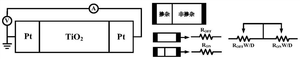
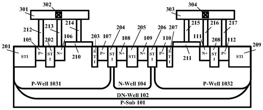
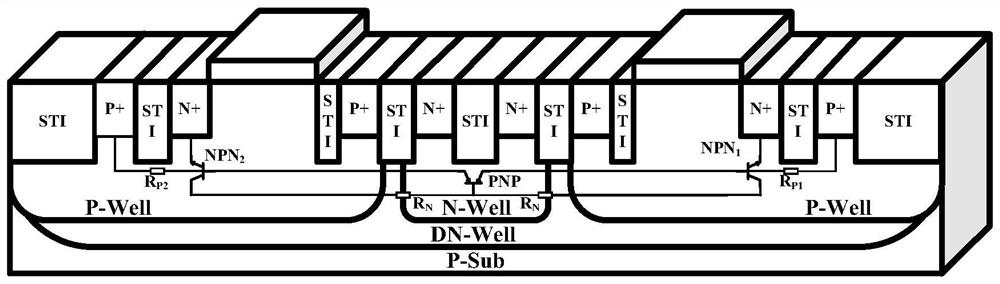
[0030] Such as Figure 2-Figure 5 As shown, a negative resistance clamp silicon controlled rectifier memristive device includes a substrate P-Sub101, and a DN-Well region 102 is provided on the substrate P-Sub101,...


PUM


Abstract

The invention discloses a negative resistance clamping silicon controlled rectifier rectification memristor and a manufacturing method thereof. A DN-Well region is arranged on a substrate P-Sub, and a first P-Well region, an N-Well region and a second P-Well region are arranged in the DN-Well region; a first shallow slot isolation region, a first P + injection region, a second shallow slot isolation region, a first N + injection region, a first polysilicon gate, a third shallow slot isolation region and a second P + injection region are arranged in the first P-Well region, and a fourth shallow slot isolation region stretches across the junction of the first P-Well region and the N-Well region; a second N + injection region, a fifth shallow slot isolation region and a third N + injection region are arranged in the N-Well region; a sixth shallow slot isolation region stretches across the junction of the N-Well region and the second P-Well region; a third P + injection region, a seventh shallow slot isolation region, a second polysilicon gate, a fourth N + injection region, an eighth shallow slot isolation region, a fourth P + injection region and a ninth shallow slot isolation region are arranged in the second P-Well region; in this way, continuous adjustment and control of the high resistance state and the low resistance state are achieved, and the requirement for large-scale on-chip integration of the silicon-based memristor based on the standard microelectronic technology is met.

Description

technical field [0001] The invention relates to the field of integrated circuits, in particular to a negative resistance clamp silicon controlled rectifier memristive device and a manufacturing method thereof. Background technique [0002] The advent of the era of artificial intelligence poses urgent problems for the computing efficiency and capacity of computer core chips. Currently, traditional chips based on the von Neumann architecture are facing severe challenges. In traditional computer architectures, computing and storage functions cannot be unified. With the continuous development of intelligent applications, the demand for data storage has shown explosive growth. In the face of increasingly complex data perception, due to the lack of breakthrough core device structures, research on artificial neural networks and artificial intelligence chips has stagnated. It is difficult for intelligent computing chips to simulate the information storage and operation of the human ...

Claims


Application Information

Patent Timeline
Patent Type & Authority Applications(China)
IPC IPC(8): H01L45/00H01L27/24
CPCH10B63/32H10N70/253H10N70/20H10N70/841H10N70/011
Inventor 金湘亮汪洋
Owner HUNAN NORMAL UNIVERSITY
Why Eureka
Try Eureka