Method for transferring two-dimensional material to hole substrate

A two-dimensional material and substrate technology, which is applied in the manufacture of electrical components, semiconductor/solid-state devices, circuits, etc., can solve the problems of weak adsorption capacity, cumbersome materials, and insufficient clean steps on the surface of materials, so as to improve the success rate and simple operation Effect

Pending Publication Date: 2021-12-28
XIAMEN UNIV
View PDF0 Cites 2 Cited by
  • Summary
  • Abstract
  • Description
  • Claims
  • Application Information

AI Technical Summary

Problems solved by technology

The surface of the material after wet transfer is not clean enough and the steps are cumbersome, while the surface of the material after dry transfer is clean and easy to op

Method used


Image

  • Method for transferring two-dimensional material to hole substrate
  • Method for transferring two-dimensional material to hole substrate

Examples


Embodiment 1

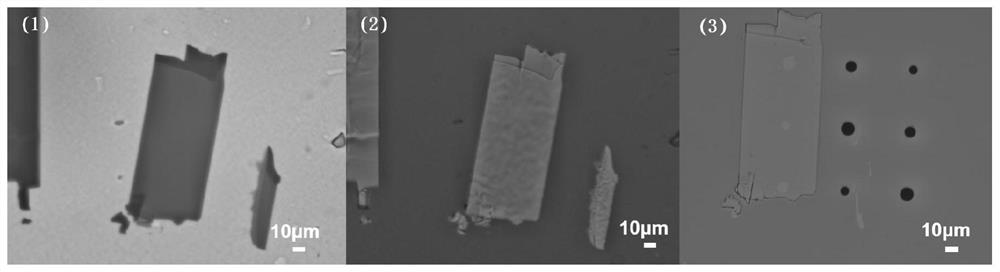
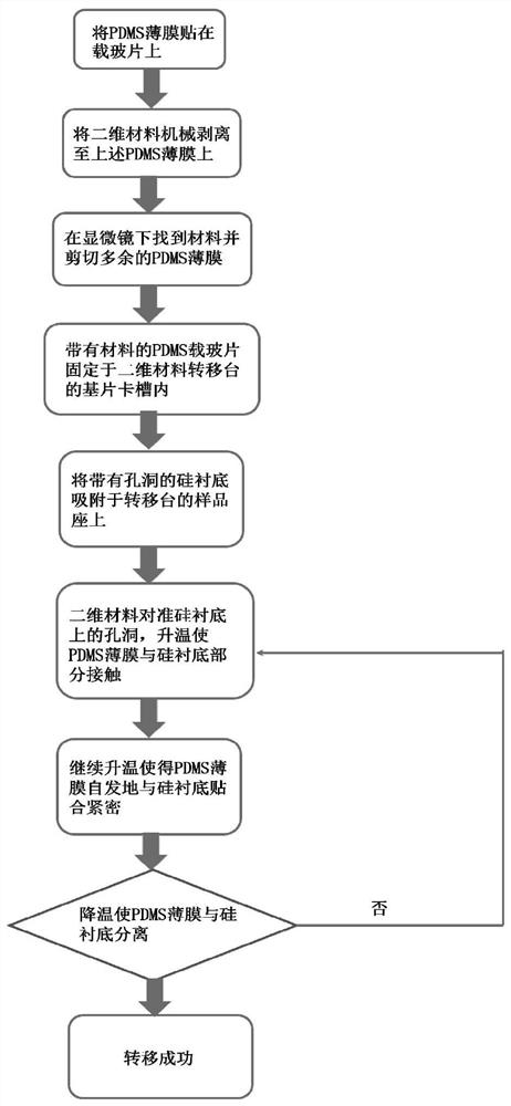
[0028] Embodiments of the present invention include the following steps:

[0029] The first step: cut the polydimethylsiloxane (Polydimethylsiloxane, PDMS) film into a size of 2 × 2cm and stick it on the glass slide;

[0030] The second step: the two-dimensional material block is folded in half on the tape several times and then mechanically peeled off to the PDMS film obtained in the first step;

[0031] Step 3: Find the material that has been mechanically peeled off in the second step under the microscope, cut off the excess PDMS film, and cut it into a size of 5×5mm;

[0032] Step 4: Fix the glass slide with material obtained in the third step in the substrate slot of the transfer table;

[0033] Step 5: Adsorb the silicon Si substrate with holes on the sample holder of the transfer table;

[0034] Step 6: Align the materials in step 4 with the holes on the Si substrate precisely, and raise the temperature to 60°C to make the PDMS film partially contact with the substrate...

Embodiment 2

[0038] The first step: cutting the polydimethylsiloxane (PDMS) film into a size of 1 × 1 cm and pasting it on a glass slide;

[0039] The second step: the two-dimensional material block is folded in half on the tape several times and then mechanically peeled off to the PDMS film obtained in the first step;

[0040] Step 3: Find the material that has been mechanically peeled off in the second step under the microscope, cut off the excess PDMS film, and cut it into a size of 3×3mm;

[0041] Step 4: Fix the glass slide with material obtained in the third step in the substrate slot of the transfer table;

[0042] Step 5: Adsorb the silicon Si substrate with holes on the sample holder of the transfer table;

[0043] Step 6: Align the materials in step 4 with the holes on the Si substrate precisely, and raise the temperature to 75°C to make the PDMS film partially contact with the substrate;

[0044] Step 7: Continue to raise the temperature to 110°C and keep it for 15 minutes to ...


PUM

PropertyMeasurementUnit
Length and widthaaaaaaaaaa
Thicknessaaaaaaaaaa
Sizeaaaaaaaaaa

Abstract

The invention discloses a method for transferring a two-dimensional material to a hole substrate, and relates to two-dimensional material transfer. The method comprises: pasting a PDMS thin film on the glass slide; stripping a two-dimensional material block onto the PDMS film; shearing the redundant part of the PDMS film under a microscope; fixing the obtained glass slide with the material in a substrate clamping groove of a two-dimensional material transfer table; adsorbing the silicon substrate with the hole on a sample seat of a transfer table; aligning the material to the hole in the Si substrate, and heating to make the PDMS film partially contact with the Si substrate; continuously raising the temperature to enable the PDMS film to be spontaneously and tightly attached to the Si substrate; and carrying out cooling to separate the PDMS film from the Si substrate. The viscosity of the PDMS film is adjusted by changing the temperature, so that the two-dimensional material is transferred to the silicon substrate with the holes. The method is a pure dry transfer method, the surface of the transferred sample is clean, the operation is simple, and the method can be realized only by controlling the temperature of the PDMS film without the help of excessive experimental instruments except a transfer table.

Description

technical field [0001] The invention relates to the technical field of two-dimensional material transfer, in particular to a method for transferring a two-dimensional material onto a hole substrate. Background technique [0002] Two-dimensional materials are materials bonded by interlayer van der Waals forces, and have broad applications in optoelectronics, electronics, and thermals. After Novoselov obtained graphene by mechanical exfoliation in 2004, more and more two-dimensional materials were discovered, including transition metal chalcogenides, black phosphorus, and boron nitride. Most two-dimensional materials are grown on substrate materials, and the transfer of two-dimensional materials is crucial for the construction of two-dimensional material heterojunctions and their devices. [0003] At present, existing transfer methods include wet transfer and dry transfer, wherein wet transfer includes substrate etching method, electrochemical bubbling method and so on. Dry ...

Claims


Application Information

Patent Timeline
IPC IPC(8): H01L21/02H01L21/027
CPCH01L21/02381H01L21/02527H01L21/02557H01L21/0272
Inventor 张学骜邓楚芸苏悦卫月华郑晓明陈扬波刘金鑫
Owner XIAMEN UNIV
Why Eureka
Try Eureka