Laser de-bonding method

A debonding and laser technology, applied in the field of laser debonding, can solve problems such as increased workload, increased cost, and cumbersome

Pending Publication Date: 2021-12-28
北京中科镭特电子有限公司
View PDF0 Cites 2 Cited by
  • Summary
  • Abstract
  • Description
  • Claims
  • Application Information

AI Technical Summary

Problems solved by technology

However, using this method requires a large number of experiments to determine the wavelength of the laser, which is cumbersome, increases the workload, and increases the cost.

Method used


Image

  • Laser de-bonding method
  • Laser de-bonding method
  • Laser de-bonding method

Examples


Embodiment Construction

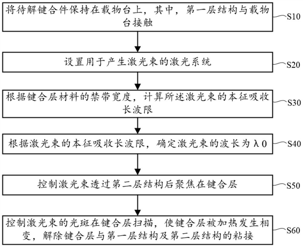
[0043]In order to make the purpose, technical solutions and advantages of the embodiments of the present invention clearer, the technical solutions in the embodiments of the present invention will be clearly and completely described below in conjunction with the drawings in the embodiments of the present invention. Obviously, the described embodiments It is only some embodiments of the present invention, but not all embodiments. Based on the embodiments of the present invention, all other embodiments obtained by persons of ordinary skill in the art without making creative efforts belong to the protection scope of the present invention.

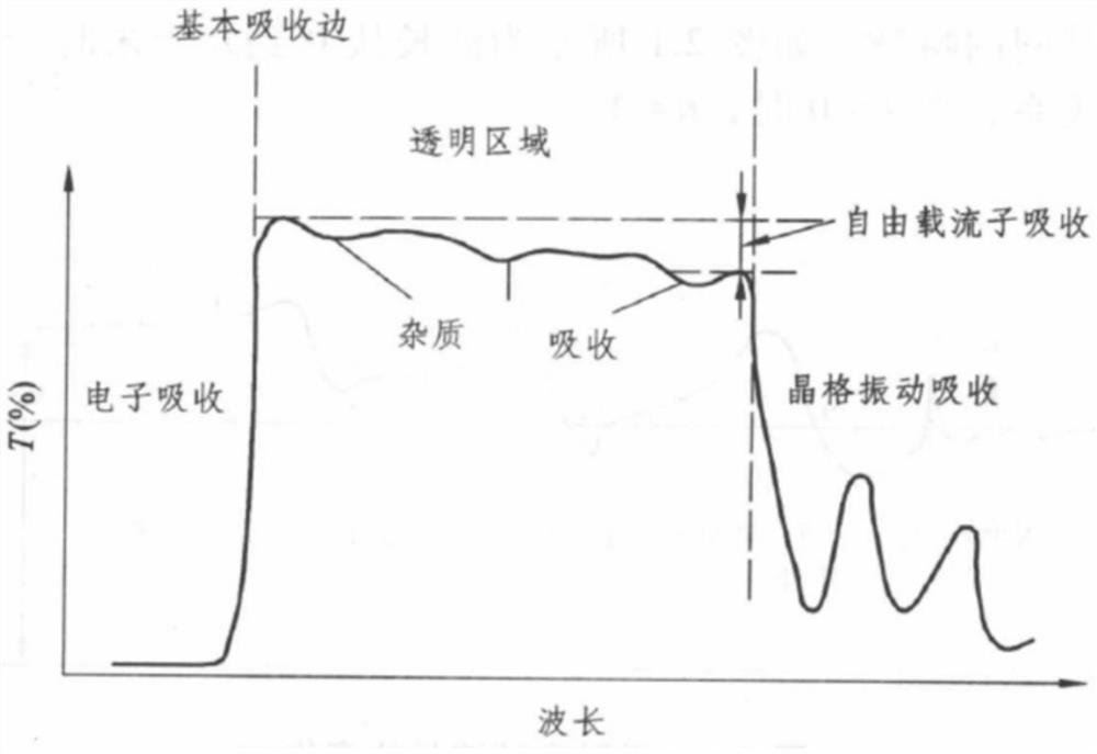
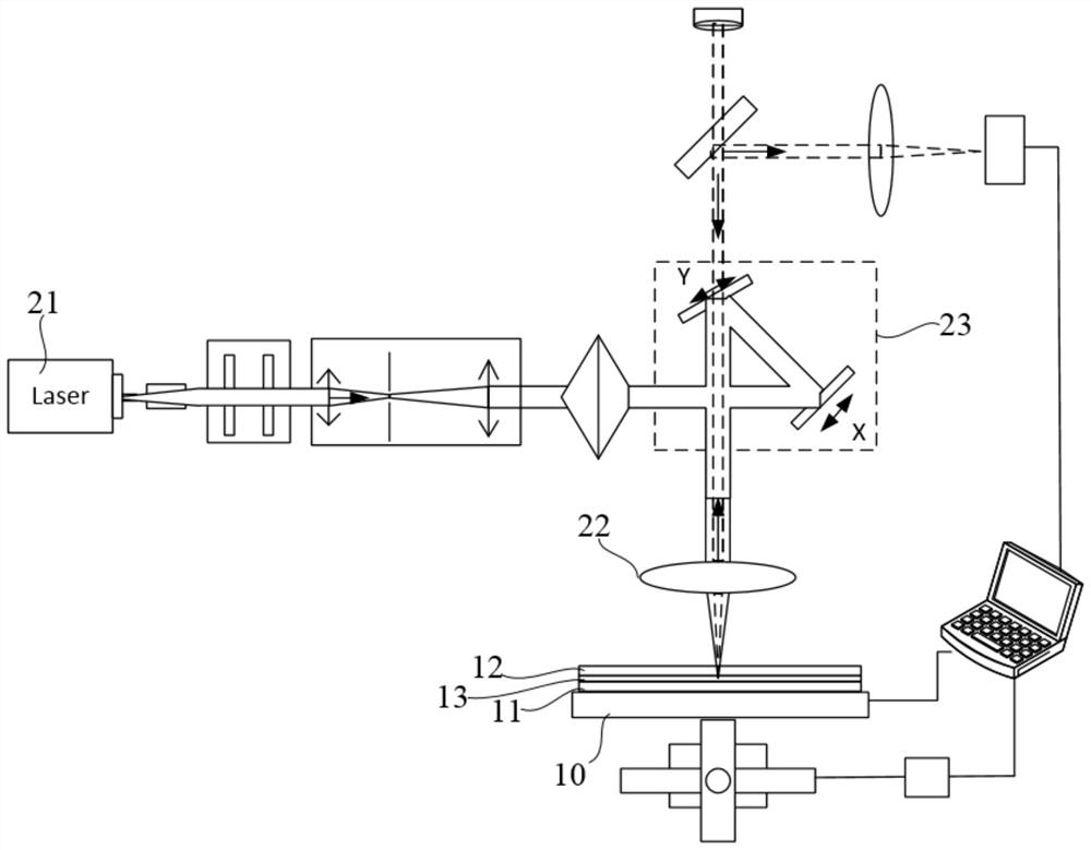
[0044] In order to facilitate the understanding of the laser debonding method provided by the embodiment of the present invention, the application scenario of the laser debonding method provided by the embodiment of the present invention is firstly described below. The debonding member includes a first layer structure and a second layer struct...


PUM


Abstract

The invention provides a laser de-bonding method. The method is used for de-bonding a to-be-de-bonded piece, and the to-be-de-bonded piece comprises a first layer structure and a second layer structure which is bonded through a bonding layer. According to the laser de-bonding method, the intrinsic absorption long wave limit of a laser beam is firstly calculated according to the forbidden band width of a bonding layer material; and then the final wavelength of the laser beam can be determined according to the intrinsic absorption long wave limit of the laser beam, so that the proper laser wavelength can be rapidly determined, the difficulty of determining the laser wavelength is simplified, the workload is reduced, and the cost is reduced. When the laser beam with the finally determined wavelength is adopted to scan the bonding layer, it can be guaranteed that the light absorption efficiency of the bonding layer is within a large interval, then the bonding layer can be heated to be in a phase change state within a short time, bonding between the bonding layer and the first layer structure and bonding between the bonding layer and the second layer structure can be rapidly removed, rapid debonding is facilitated, and the de-bonding efficiency is improved.

Description

technical field [0001] The invention relates to the technical field of semiconductor manufacturing, in particular to a laser debonding method. Background technique [0002] In the manufacturing process of the chip, a large number of microelectronic devices are usually processed on the wafer by means of etching, deposition, polishing, etc. A wafer is a thin slice cut from a single crystal silicon ingot, and its thickness is usually between 0.3mm and 0.9mm, which shows that the thickness is very thin. Since the thickness of the wafer is relatively thin, and when various circuits are processed on the wafer, multiple times of etching, polishing, cleaning, etc. are required. Usually, the wafer is temporarily bonded to the substrate before processing. Afterwards, processes such as deposition and etching are carried out on the surface of the wafer to manufacture various microelectronic devices on the surface of the wafer. After the wafer processing is completed, the wafer and the...

Claims


Application Information

Patent Timeline
Patent Type & Authority Applications(China)
IPC IPC(8): H01L21/68H01L21/683H01L21/67
CPCH01L24/799H01L21/6838H01L21/681H01L2224/7999
Inventor 李纪东张紫辰侯煜张昆鹏张喆张彪易飞跃杨顺凯
Owner 北京中科镭特电子有限公司
Why Eureka
Try Eureka