
Infrared detector mirror pixel and infrared detector based on cmos technology

An infrared detector and process technology, applied in the field of infrared detection, can solve the problems of low yield rate, low pixel scale, and low performance of infrared detectors, and achieve the effect of reducing transportation costs, reducing transportation, and not being limited by technology

Active Publication Date: 2022-12-02
BEIJING NORTH GAOYE TECH CO LTD
View PDF3 Cites 0 Cited by
  • Summary
  • Abstract
  • Description
  • Claims
  • Application Information

AI Technical Summary

Problems solved by technology

[0012] In order to solve the above-mentioned technical problems or at least partly solve the above-mentioned technical problems, the present disclosure provides an infrared detector image element and an infrared detector based on CMOS technology, which can solve the problem of low performance and low pixel scale of traditional MEMS technology infrared detectors. , low yield and other issues

Method used


Image

  • Infrared detector mirror pixel and infrared detector based on cmos technology
  • Infrared detector mirror pixel and infrared detector based on cmos technology
  • Infrared detector mirror pixel and infrared detector based on cmos technology

Examples


Embodiment Construction

[0097] In order to understand the above-mentioned purpose, features and advantages of the present invention more clearly, the solutions of the present invention will be further described below. It should be noted that, in the case of no conflict, the embodiments of the present invention and the features in the embodiments can be combined with each other.

[0098] In the following description, many specific details have been set forth in order to fully understand the present invention, but the present invention can also be implemented in other ways different from those described here; obviously, the embodiments in the description are only some embodiments of the present invention, and Not all examples.

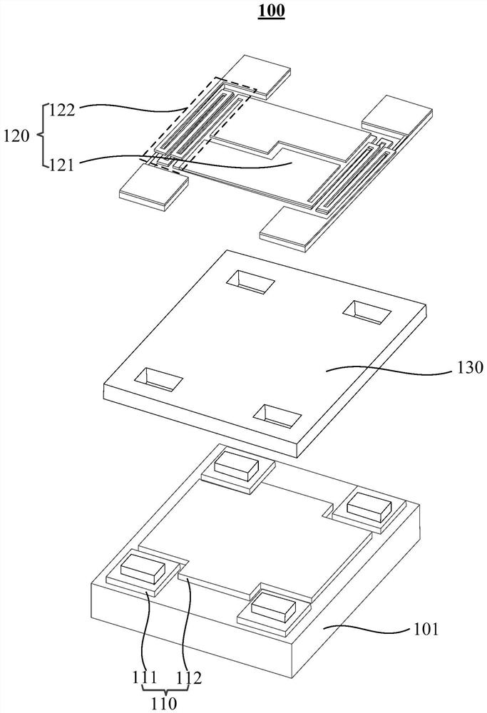
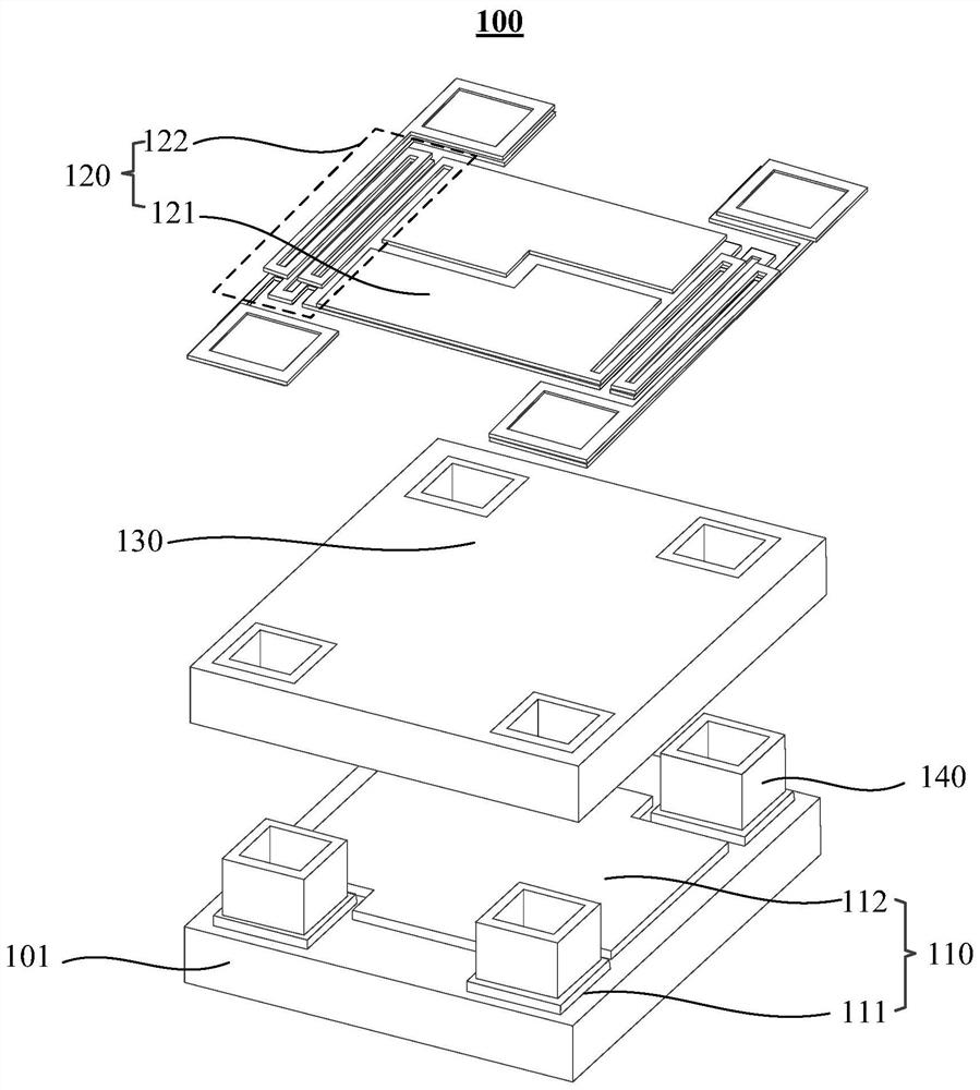
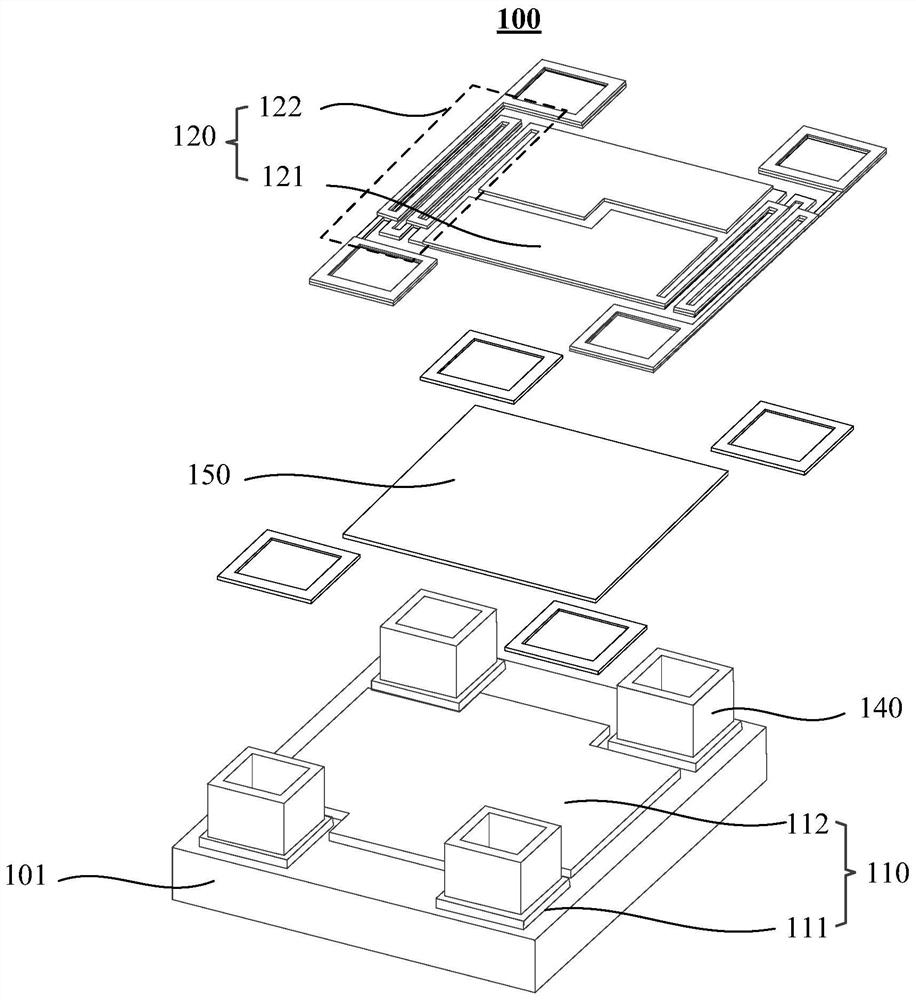
[0099] figure 1 A schematic diagram of a three-dimensional decomposition structure of an infrared detector image element based on a CMOS process provided by an embodiment of the present invention, figure 2 A schematic diagram of a three-dimensional decomposition structure of...


PUM


Abstract

This openness involves an infrared detector mirror image based on CMOS technology.CMOS infrared sensor structure; CMOS infrared sensor structure includes reflex layers and infrared conversion structures. The infrared conversion structure is connected to the CMOS measurement circuit system by supporting the base.At least one type in titanium oxide is not formed between the CMOS measurement circuit system and the infrared conversion structure, or the resonant cavity formed cannot reflect infrared light to the infrared conversion structure, or the infrared conversion structure reflects infrared light.Through this open technical solution, the problem of low performance, low pixel scale, and low yield of infrared detectors of traditional MEMS process are solved.

Description

technical field [0001] The present disclosure relates to the technical field of infrared detection, and in particular to an infrared detector mirror image element and an infrared detector based on a CMOS process. Background technique [0002] Surveillance market, automotive auxiliary market, home furnishing market, intelligent manufacturing market, and mobile phone applications all have strong demand for uncooled high-performance chips, and have certain requirements for chip performance, performance consistency, and product prices. It is estimated that there is a potential demand of more than 100 million chips every year, but the current process scheme and architecture cannot meet the market demand. [0003] At present, the infrared detector adopts the method of combining the measurement circuit and the infrared sensing structure. The measurement circuit is prepared by CMOS (Complementary Metal-Oxide-Semiconductor, Complementary Metal Oxide Semiconductor) technology, and the...

Claims


Application Information

Patent Timeline
Patent Type & Authority Patents(China)
IPC IPC(8): G01J5/10G01J5/20G01J5/24G01J5/58G01J5/00G01J5/068
CPCG01J5/10G01J5/20G01J5/24G01J5/58G01J5/00G01J2005/103G01J2005/106G01J2005/202G01J2005/0077Y02P70/50
Inventor 翟光杰武佩潘辉翟光强
Owner BEIJING NORTH GAOYE TECH CO LTD
Learn More