Heat conduction structure and manufacturing method thereof, heat conduction system, chip packaging structure and electronic equipment

A heat-conducting structure and heat-conducting film technology are used in heat-conducting systems, heat-conducting structures and manufacturing methods thereof, and electronic equipment fields, and can solve the problem of high junction temperature of layered chips

Pending Publication Date: 2022-01-04
HUAWEI TECH CO LTD
View PDF0 Cites 0 Cited by
  • Summary
  • Abstract
  • Description
  • Claims
  • Application Information

AI Technical Summary

Problems solved by technology

[0005] Embodiments of the present application provide a heat conduction structure and its manufacturing method, heat conduction system, chip packaging structure, and electronic equipment, which improve the bonding strength between the heat conduction structure, heating elements, and radiators, and reduce the heat dissipation of the heat conduction structure, heat generating elements, and heat dissipation. The contact thermal resistance between the heat sinks improves the heat conduction effect of the heat conduction structure, and solves the problem that the existing heat conduction pad and the chip and / or heat sink are prone to delamination and cause the chip junction temperature to be too high

Method used


Image

  • Heat conduction structure and manufacturing method thereof, heat conduction system, chip packaging structure and electronic equipment
  • Heat conduction structure and manufacturing method thereof, heat conduction system, chip packaging structure and electronic equipment
  • Heat conduction structure and manufacturing method thereof, heat conduction system, chip packaging structure and electronic equipment

Examples


Embodiment 1

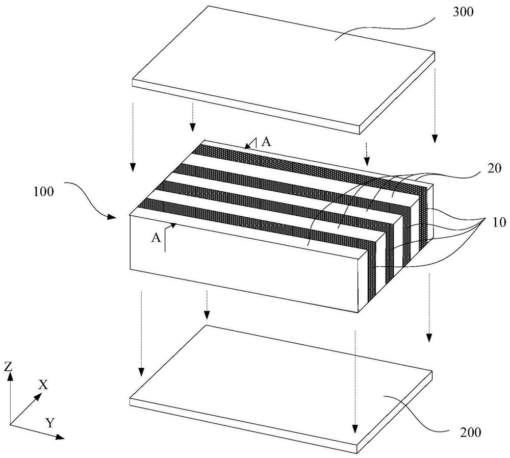
[0109] The heat conduction structure 100 provided by the embodiment of the present application can transfer the heat generated by the heating element 200 to the heat sink 300, see figure 1 As shown, the heat conducting structure 100 is located between the heating element 200 and the radiator 300, according to figure 1 After the arrow in the figure is assembled, one side of the heat conducting structure 100 is in contact with the heating element 200, and the other side of the heat conducting structure 100 can be in contact with the heat sink 300, so that the heat generated by the heating element 200 is transferred to the heat sink 300 through the heat conducting structure 100, thereby realizing the Heat dissipation of the heating element 200.

[0110] Wherein, the heating element 200 may be a chip or an electronic component that generates heat. In the embodiment of the present application, the heating element 200 is a chip as an example for illustration. The heat sink 300 can ...

Embodiment 2

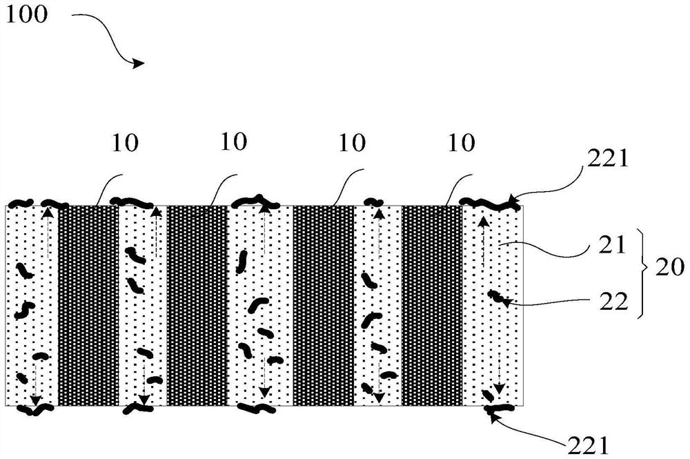
[0191] The difference from the above embodiment is that in the embodiment of the present application, the second organic material 22 can be generated between the heat generating structure 200 and the heat conducting structure 100 and / or between the heat conducting structure 100 and the radiator 300 under preset reaction conditions. Polymerized materials. Moreover, the adhesive layer 221 formed after the polymerization reaction of the second organic material 22 has pressure-sensitive properties. That is, the generated adhesive layer 221 is a pressure-sensitive adhesive, so that by applying pressure to the heating element 200 and the heat sink 300, the heat conducting structure 100 and the heating element 200 and / or the heat conducting structure 100 and the heat sink 300 Close adhesion is achieved through the formed adhesive layer 221 .

[0192] The polymerization reaction of the second organic material 22 between the heat generating structure 200 and the heat conducting struct...

Embodiment 3

[0205] The embodiment of the present application also provides a method for manufacturing the heat conduction structure 100, such as Figure 6 As shown, the method includes the following steps:

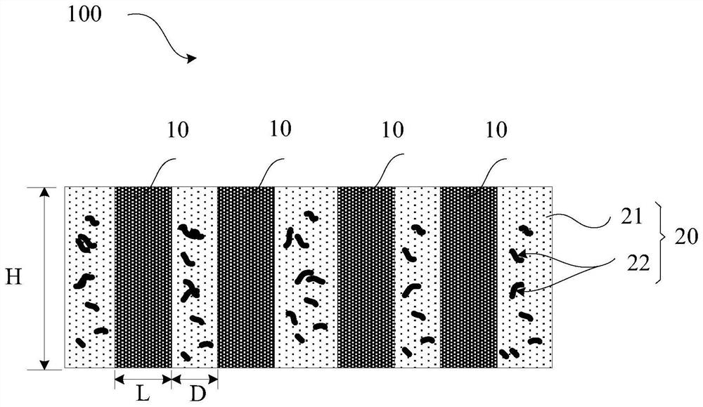
[0206] S101. Provide a plurality of thermally conductive films 10, each thermally conductive film 10 has a first surface 11 and a second surface 12 opposite to the first surface 11;

[0207] see Figure 7A As shown, four thermally conductive films 10 are provided. Certainly, in some other examples, the number of the heat conduction film 10 includes but is not limited to four. The heat conduction film 10 can be a graphene film or an artificial graphite film.

[0208] Wherein, when the thermally conductive film 10 is a graphene film, the preparation method is as follows: use a single-layer graphene oxide microchip whose D50 size is 20 μm (that is, the longitudinal dimension of the graphene microchip is 20 μm), and weigh 500 mg of a single-layer graphene oxide microchip. The tablets ...


PUM


Abstract

The embodiment of the invention provides a heat conduction structure and a manufacturing method thereof, a heat conduction system, a chip packaging structure and electronic equipment. According to the invention, a second organic material in the heat conduction structure is diffused to the outer surface of the heat conduction structure, the second organic material diffused outwards forms a bonding layer between the heat conduction structure and a heating element and / or between the heat conduction structure and a radiator, and the bonding layer connects the heat conduction structure with the heating element and / or connects the heat conduction structure with the radiator, so that the heat conduction structure is ensured to be in close contact with the surface of the heating element / radiator so as to avoid the problem of overtemperature of the heating element caused by layering of an interface between the heat conduction structure and the heating element / radiator in the use process; and local micropores between the heat conduction structure and the heating element and between the heat conduction structure and the radiator can be filled with the second organic material which diffuses outwards, so that the micro wettability of the heat conduction structure is improved so as to reduce the interface contact thermal resistance and reduce the application thermal resistance of the heat conduction structure.

Description

technical field [0001] The embodiments of the present application relate to the technical field of heat conduction, and in particular to a heat conduction structure and a manufacturing method thereof, a heat conduction system, a chip packaging structure and electronic equipment. Background technique [0002] As electronic devices continue to integrate more powerful functions into smaller components, temperature control has become one of the critical challenges in design, that is, how to effectively take away More heat generated by greater unit power is an urgent problem to be solved. [0003] At present, the heat generated by the chip is mainly transferred to the radiator through the thermal pad to dissipate heat from the chip. Specifically, the thermal pad is placed on the chip, and the other side of the thermal pad away from the chip is connected to the radiator. The pad and the thermal pad are connected to the heat sink with an adhesive layer. [0004] However, during t...

Claims


Application Information

Patent Timeline
Patent Type & Authority Applications(China)
IPC IPC(8): H01L23/367H01L23/373
CPCH01L23/3672H01L23/3735H01L23/3737H01L23/3675
Inventor 徐焰王奋成赵仁哲
Owner HUAWEI TECH CO LTD
Why Eureka
Try Eureka