Light emitting diode and light emitting device

A technology of light-emitting diodes and connecting electrodes, which is applied to semiconductor devices, electrical components, circuits, etc., can solve the problems of weakened heat dissipation, high void rate in pad electrode area, and reduced thrust, so as to improve reliability, avoid water vapor intrusion, The effect of improving the cooling capacity

Active Publication Date: 2022-01-07
XIAMEN SANAN OPTOELECTRONICS CO LTD
View PDF20 Cites 1 Cited by
  • Summary
  • Abstract
  • Description
  • Claims
  • Application Information

AI Technical Summary

Problems solved by technology

This leads to some problems, such as: after the client die-bonding, the pad electrode area with a significant difference in height has a high void rate, which leads to a decrease in thrust and a weakened heat dissipation capability, and during or after the die-bonding process, the external force Acting on the chip, the insulating layer is easily broken because of its brittleness, which leads to the connection between the upper and lower metal layers with different electrical polarities and a local short circuit phenomenon.

Method used

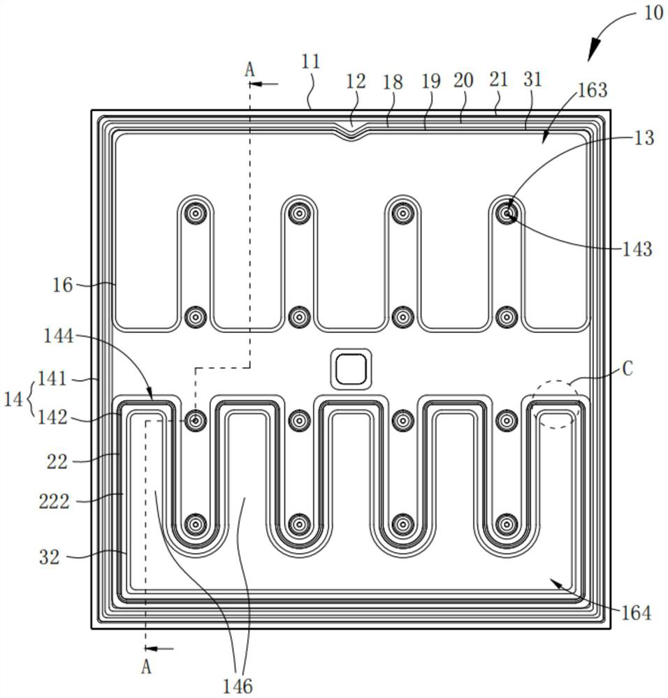
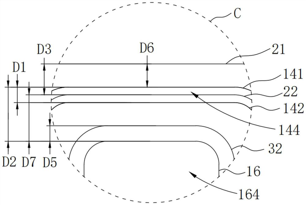
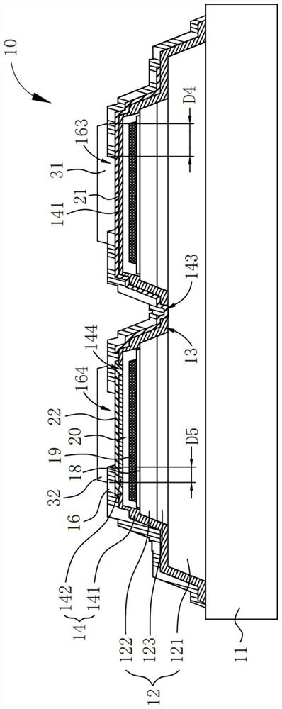

Image

  • Light emitting diode and light emitting device
  • Light emitting diode and light emitting device
  • Light emitting diode and light emitting device

Examples


Embodiment Construction

[0040] In order to make the purpose, technical solutions and advantages of the embodiments of the present invention clearer, the technical solutions in the embodiments of the present invention will be clearly and completely described below in conjunction with the drawings in the embodiments of the present invention. Obviously, the described embodiments It is a part of the embodiments of the present invention, rather than all embodiments; the technical features designed in the different embodiments of the present invention described below can be combined as long as they do not constitute conflicts; based on the embodiments of the present invention, the present invention All other embodiments obtained by persons of ordinary skill in the art without creative efforts fall within the protection scope of the present invention.

[0041] In describing the present invention, it should be understood that the terms "central", "lateral", "upper", "lower", "left", "right", "vertical", "hori...


PUM

PropertyMeasurementUnit
thicknessaaaaaaaaaa

Abstract

The invention provides a light-emitting diode, which comprises an epitaxial structure, a via hole, a first insulating layer, a connecting electrode, a second insulating layer and bonding pads. The epitaxial structure comprises a first semiconductor layer, a light-emitting layer and a second semiconductor layer which are stacked in sequence; the first insulating layer comprises a first insulating part and a second insulating part which cover the second semiconductor layer, the first insulating part further extends to the bottom of the via hole, and the second insulating part and the first insulating part are spaced through an annular second opening; the first connection electrode is electrically connected with the first semiconductor layer through the first opening; the second connection electrode is electrically connected with the second semiconductor layer through the second opening; the second insulating layer is positioned on the first connecting electrode and the second connecting electrode and is provided with a third opening and a fourth opening; the first bonding pad is electrically connected with the first connecting electrode through the third opening; and the second bonding pad is electrically connected with the second connection electrode through the fourth opening. Therefore, the heights of the two bonding pads can be consistent, and a light-emitting diode with high height consistency is obtained.

Description

technical field [0001] The invention relates to the technical field of light-emitting diode manufacturing, in particular to a light-emitting diode and a light-emitting device with high uniformity. Background technique [0002] Light Emitting Diode (English: Light Emitting Diode, referred to as: LED) has the advantages of low cost, high luminous efficiency, energy saving and environmental protection, and is widely used in lighting, visible light communication, and light-emitting display and other scenarios. LED chips are divided into three types: positive structure, flip structure and vertical structure. Compared with the traditional front-mounted chip, the flip-chip LED chip structure is to invert the diode structure, emit light from the sapphire side, and the electrode side can be fixed on the substrate with better heat dissipation. [0003] The current flip-chip LED chip structure is divided into a metal reflective layer or an insulating reflective layer on the epitaxial ...

Claims


Application Information

Patent Timeline
Patent Type & Authority Applications(China)
IPC IPC(8): H01L33/38H01L33/10
CPCH01L33/38H01L33/10H01L33/382H01L33/405H01L33/42H01L33/44H01L33/62
Inventor 朱秀山李燕
Owner XIAMEN SANAN OPTOELECTRONICS CO LTD
Why Eureka
Try Eureka