Terahertz dual-channel modulator and preparation method thereof
A dual-channel, modulator technology, applied in the field of microwave transmission, can solve the problems of inability to independently modulate communication technologies, and achieve the effects of small size, easy integration, and high modulation depth
- Summary
- Abstract
- Description
- Claims
- Application Information
AI Technical Summary
Problems solved by technology
Method used
Image

Examples
Embodiment 1
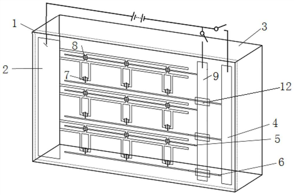
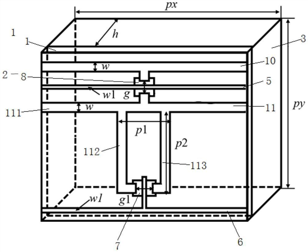
[0046] This embodiment discloses a terahertz dual-channel modulator, such as figure 1 and image 3 As shown, it includes a substrate 3, an epitaxial layer 1 and a modulation array, the epitaxial layer 1 is grown on the substrate 3, and the modulation array is arranged on the epitaxial layer 1;
[0047] The modulation array is composed of M*N array element structures, and the array element structures are arranged in an array, and the first grid feeder 5 and the first Schottky electrode 9 of each row of array element structures connection, the second gate feeder 6 of each row of array element structure is connected to the second Schottky electrode 4, M>2, N>2; the first source-drain feeder 10 of each row of array element structure The second source-drain feeder 11 is connected to the ohmic electrode 2; the modulation array is used to pass terahertz waves of different frequencies; the first Schottky electrode 9 is connected to the second Schottky electrode 4 are respectively co...
Embodiment 2
[0063] This embodiment discloses a method for preparing a terahertz dual-channel modulator, and the steps of the preparation method include:
[0064] S1: cleaning the substrate 3 by means of ultrasonic cleaning, and drying the cleaned substrate 3;
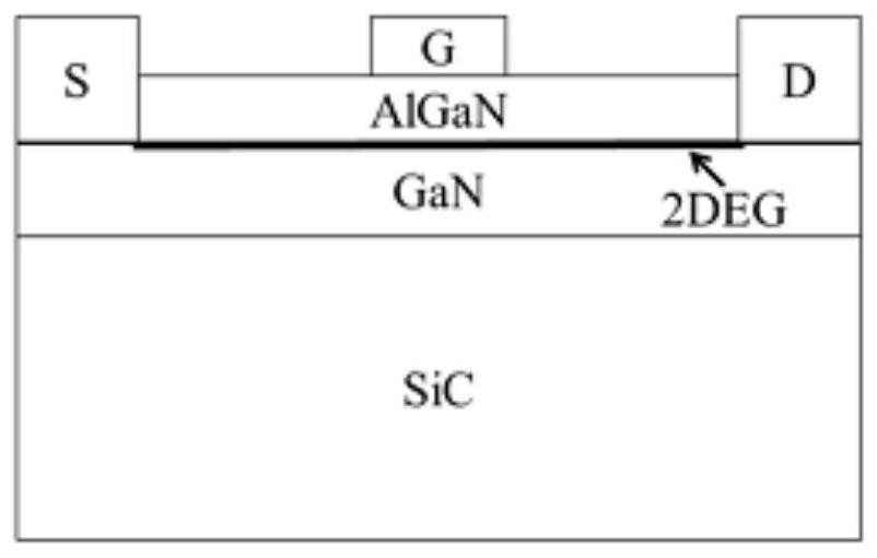
[0065] S2: preparing an AlGaN / GaN heterojunction thin film on the substrate 3 by using an organic compound vapor deposition method to obtain a substrate;
[0066] S3: Spin-coat a 2 μm thick photoresist on the substrate, use a mask to develop photolithography, determine the HEMT active area, and use inductively coupled plasma etching to etch away the AlGaN / GaN thin film, remove the remaining photoresist on the substrate to obtain the HEMT active region substrate;
[0067]Preparation of the HEMT active region. First, spin-coat a photoresist with a thickness of 2 μm on the substrate, and use a mask for photolithography development to determine the active region of the HEMT. Then, the AlGaN / GaN film outside the active region of the...
PUM
| Property | Measurement | Unit |
|---|---|---|
| Thickness | aaaaa | aaaaa |
Abstract
Description
Claims
Application Information
 - R&D
- Intellectual Property
- Life Sciences
- Materials
- Tech Scout
- Unparalleled Data Quality
- Higher Quality Content
- 60% Fewer Hallucinations
Browse by: Latest US Patents, China's latest patents, Technical Efficacy Thesaurus, Application Domain, Technology Topic, Popular Technical Reports.
© 2025 PatSnap. All rights reserved.Legal|Privacy policy|Modern Slavery Act Transparency Statement|Sitemap|About US| Contact US: help@patsnap.com