

Transparent conductive electrode, preparation method thereof, and electronic device
A transparent conductive electrode and transparent conductive technology, which is applied in the manufacture of semiconductor devices, electrical components, cables/conductors, etc., can solve the problems of increasing the resistance of transparent electrodes, affecting the photoelectric conversion efficiency of solar cells, and limiting application scenarios, so as to reduce the square resistance. Effect
Active Publication Date: 2022-01-14
HUAWEI TECH CO LTD
View PDF8 Cites 1 Cited by
- Summary
- Abstract
- Description
- Claims
- Application Information
AI Technical Summary
Problems solved by technology
[0002]Transparent conductive electrodes (also referred to as transparent electrodes) are widely used in photoelectric conversion, information display, solid-state lighting and other fields based on their own light transmission properties. Some transparent electrodes are mostly made of transparent conductive oxide (TCO). Due to the relatively high resistivity of TCO, the square resistance of the formed transparent electrode is relatively large, especially for flexible substrate scenarios. The square resistance of transparent electrodes can generally reach tens of ohms or even hundreds of ohms, resulting in a substantial increase in the resistance of large-area transparent electrodes, which in turn causes the problem of limited application of transparent electrodes.
[0003]Taking the application of transparent electrodes in solar cells (also called photovoltaic cells) as an example, transparent electrodes are an important part of solar cells, due to the square resistance of transparent electrodes If it is too high, it will seriously affect the photoelectric conversion efficiency of the solar cell. A large-area solar cell usually adopts the arrangement of multiple narrow strip-shaped sub-cells in series, resulting in lines visible to the human eye on the solar cell itself, which greatly affects its application scenarios. For example, for the current smart wearable field, consumer electronics and other electronic products, there are high requirements for vision and aesthetics, and the current solar cells that use multiple narrow strip sub-cells in series cannot meet their needs; Therefore, it is necessary to design a transparent electrode with low square resistance to expand the application scenarios of solar cells
Method used
View moreImage
Smart ImageViewing Examples

Examples
preparation example Construction
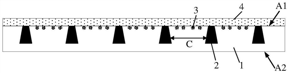
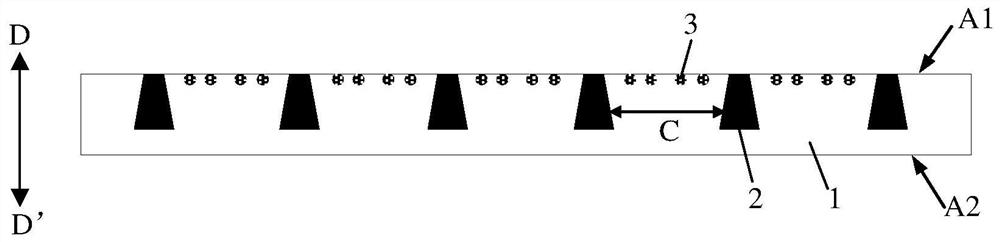
[0060] The embodiment of the present application also provides a preparation method of a transparent conductive electrode, such as Figure 4 Shown, this preparation method comprises:
[0061] Step 01. Reference Figure 5 As shown in (a), the glue layer 11 is formed on the substrate 10 .
[0062] Of course, before the gel layer 11 is formed on the substrate 10 , the substrate 10 generally needs to be cleaned, dried and so on.
Login to View More PUM
| Property | Measurement | Unit |
|---|---|---|
| thickness | aaaaa | aaaaa |
| thickness | aaaaa | aaaaa |
| thickness | aaaaa | aaaaa |
Abstract
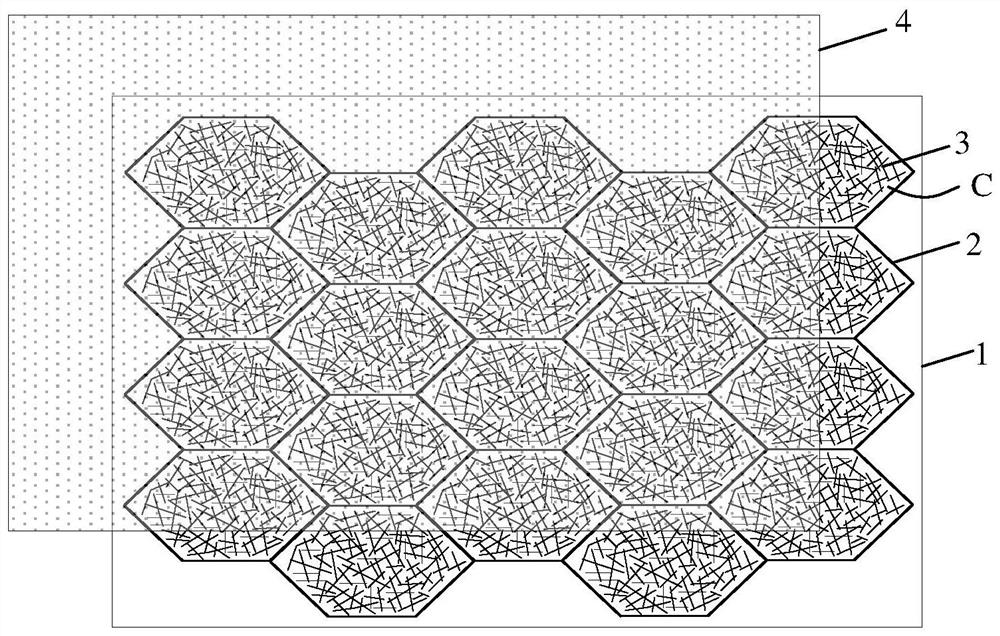
The invention provides a transparent conductive electrode, a preparation method thereof, and an electronic device, and relates to the technical field of transparent conduction. The sheet resistance of the transparent conductive electrode is reduced. The transparent conductive electrode comprises a transparent substrate, a metal grid and a metal nanowire network, wherein the metal grid and the metal nanowire network are embedded in the transparent substrate; the metal nanowire network is located in a mesh area of the metal grid; the transparent substrate comprises a first surface located in the thickness direction; the metal grid and the metal nanowire network are exposed out of the first surface and are flush with the first surface; the transparent conductive electrode further comprises a transparent conductive modification layer; and the transparent conductive modification layer covers the first surface and the metal grid and the metal nanowire network exposed out of the first surface.
Description
technical field [0001] The present application relates to the technical field of transparent conduction, in particular to a transparent conduction electrode, a preparation method thereof, and an electronic device. Background technique [0002] Transparent conductive electrodes (also referred to simply as transparent electrodes) are widely used in fields such as photoelectric conversion, information display, and solid-state lighting based on their own light transmittance. Most of the existing transparent electrodes use transparent conductive oxide (transparent conductive oxide) , TCO), due to the relatively high resistivity of TCO, the square resistance of the formed transparent electrode is relatively large, especially for the flexible substrate scenario, the square resistance of the transparent electrode can generally reach tens of ohms or even hundreds of ohms , so that the resistance of the large-area transparent electrode will be greatly increased, and then the applicati...
Claims
Login to View More Application Information
Patent Timeline
 Patent Type & AuthorityApplications(China)
IPC IPC(8): H01B5/14H01B1/02H01B13/00H01L31/0224H01L31/18B82Y30/00B82Y40/00
CPCH01B5/14H01B1/02H01B13/00H01L31/022425H01L31/022466H01L31/1884B82Y30/00B82Y40/00H01L31/0224H01L31/18Y02P70/50
Inventor王硕辛凯刘云峰
OwnerHUAWEI TECH CO LTD