
Semiconductor processing plastic packaging machine

A plastic sealing machine and semiconductor technology, applied in semiconductor/solid-state device manufacturing, electrical components, circuits, etc., can solve problems such as easy generation of air bubbles, delamination of raw materials and semiconductors, etc., to avoid wrinkles, reduce possibilities, and reduce energy consumption Effect

Pending Publication Date: 2022-01-21
尼玛东主
View PDF1 Cites 0 Cited by
  • Summary
  • Abstract
  • Description
  • Claims
  • Application Information

AI Technical Summary

Problems solved by technology

[0006] Aiming at the deficiencies of the prior art, the present invention provides a semiconductor processing plastic sealing machine, which solves the problem that during the use of the existing semiconductor processing plastic sealing machine, bubbles are easily generated between the raw materials for plastic packaging and the semiconductor when they are bonded to each other, resulting in Subsequent synergistic factors such as hydrothermal stress occurred, and the plastic-encapsulated raw materials and semiconductors were prone to delamination and detachment.

Method used


Image

  • Semiconductor processing plastic packaging machine
  • Semiconductor processing plastic packaging machine
  • Semiconductor processing plastic packaging machine

Examples


Embodiment 1

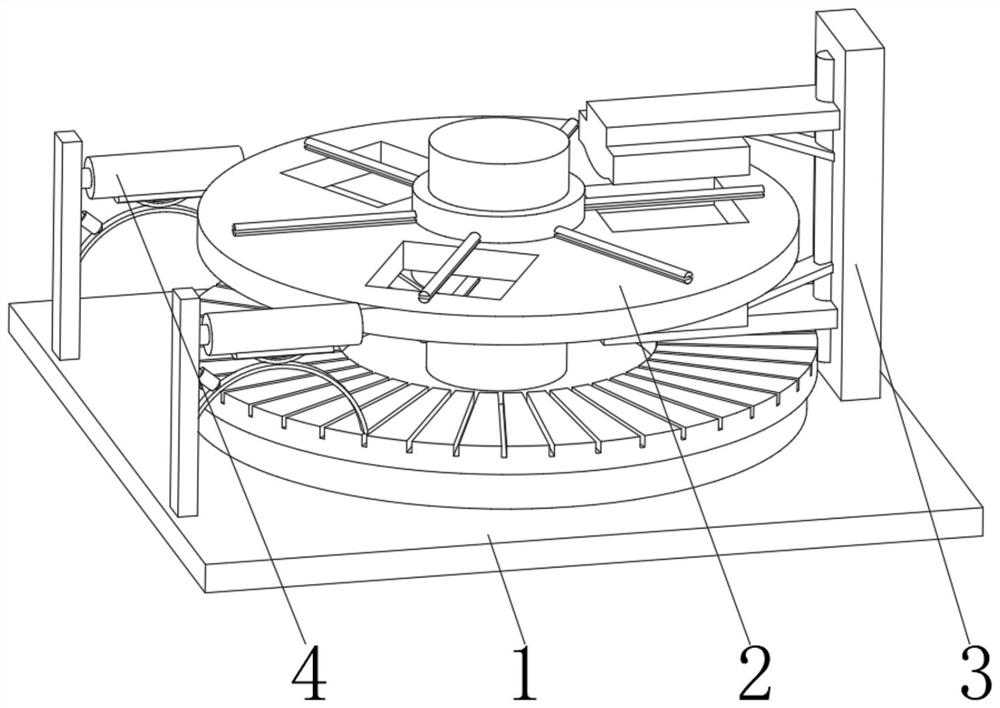
[0037] see Figure 1-3 , the present invention provides a technical solution: a semiconductor processing plastic sealing machine, specifically comprising:

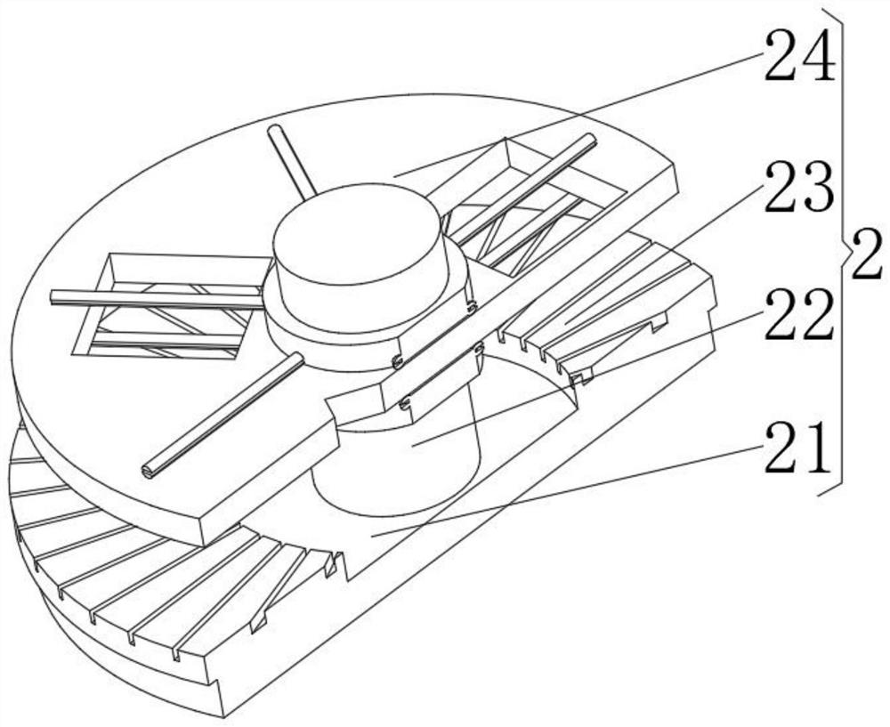
[0038] Base plate 1, the base plate 1 has a square seat plate, and a plastic sealing platform 2 installed in the middle of the top of the square seat plate, and a heat pressing mechanism 3 installed on the right side of the top of the square seat plate, and installed on the left side of the top of the square seat plate The feeding mechanism 4 at the front and back positions of the side, and the plastic sealing platform 2 include:

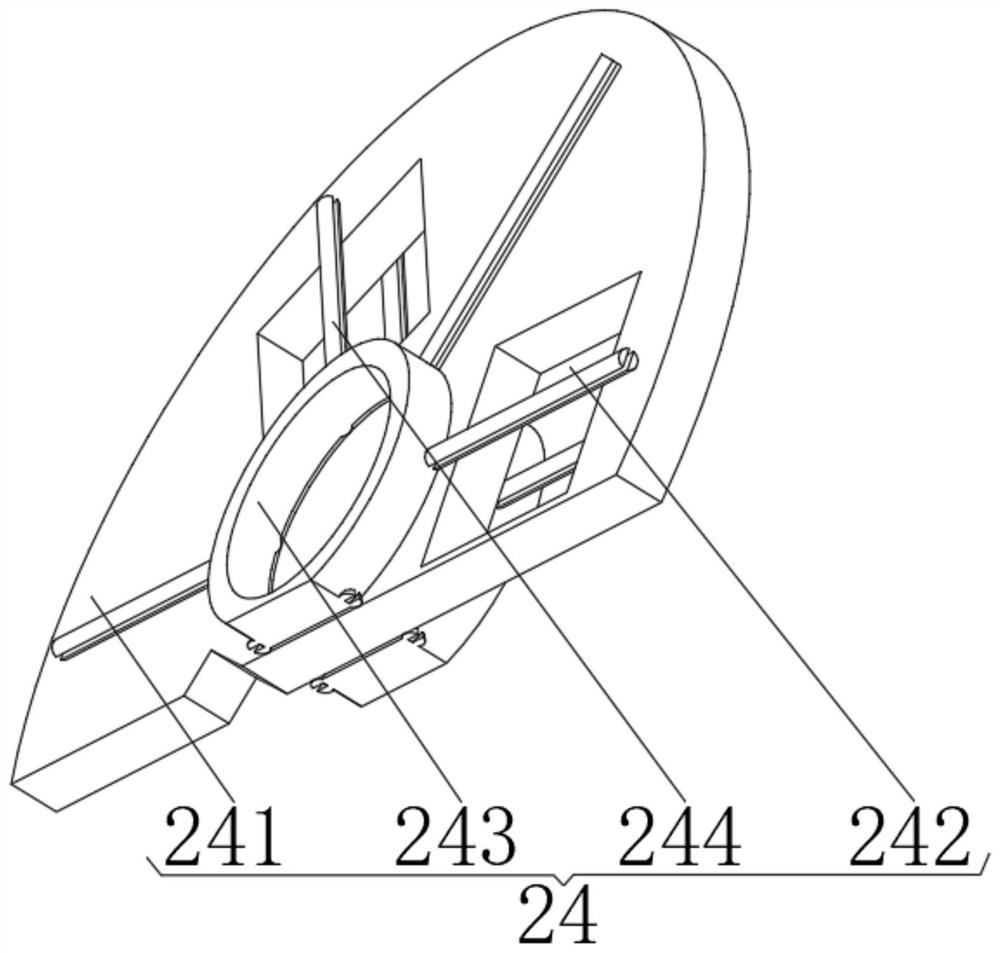
[0039] Electromagnetic plate 21, the electromagnetic plate 21 has an annular plate body, and a multi-section driving column 22 installed on the inner surface of the annular plate body, and a friction power generation ring plate 23 installed on the outer surface of the top of the annular plate body, and installed on the outer surface of the multi-section driving column 22 The object stage 24 of ...

Embodiment 2

[0046] see Figure 1-4 , On the basis of Embodiment 1, the present invention provides a technical solution: the hot pressing mechanism 3 includes:

[0047] A positioning frame 31, the positioning frame 31 has a rectangular plate body, and a track column 32 installed in the middle of the side of the rectangular plate body close to the plastic sealing platform 2, and a splint 33 installed on the outer surface of the track column 32, and installed on the inner surface of the splint 33 The heat press 34 on the side away from the track column 32 is installed on the cylinder contact plate 35 on the side of the heat press 34 away from the splint 33. The splint 33 is set as a molded plate body, and the bottom of the positioning frame 31 is installed on the base plate 1 top. Through the design of the cylindrical contact plate 35, the plastic raw materials and semiconductors are plastic-encapsulated from the inside to the outside, and the internal air is discharged in advance by using ...

Embodiment 3

[0050] see Figure 1-5 , on the basis of Embodiment 1 and Embodiment 2, the present invention provides a technical solution: the feeding mechanism 4 includes:

[0051] Fixed plate 41, the fixed plate 41 has a long strip body, and the feeding shaft column 42 installed on the top of the strip body, and the adjustment column rod installed on the surface of the strip body and positioned directly below the feeding shaft column 42 43, and the arc strut 44 that is installed on the other end of the adjustment pole 43, and the reverse arc bar 45 that is fixed on the top of the arc strut 44, and the flat plate 46 that is fixed on the reverse arc bar 45. Through the design of the leveling plate 46, the height of the plastic raw material is limited horizontally to avoid the change of the horizontal height due to the consumption of the plastic raw material roll, and at the same time, the plastic raw material is flattened to ensure the smoothness of the plastic raw material surface.

[005...


PUM


Abstract

The invention discloses a semiconductor processing plastic packaging machine which specifically comprises a base plate which is provided with a square base plate, a plastic packaging platform installed in the middle of the top of the square base plate, a hot pressing mechanism installed on the right side of the top of the square base plate, and a feeding mechanisms installed on the front face and back face of the left side of the top of the square base plate. The plastic packaging platform comprises a plurality of sections of driving columns mounted on the inner surface of the annular plate body, a friction power generation annular plate mounted on the outer side of the top of the annular plate body, and an objective table arranged at the middle upper position of the outer surface of the multi-section driving columns. The invention relates to the technical field of semiconductors. Through the design of a positioning magnetic clamping rod, the plastic raw material for plastic package is clamped and located, the dislocation change of the position during processing is avoided, the consistency between the plastic raw material and a semiconductor is ensured, meanwhile, the plastic raw material is tensioned by the positioning magnetic clamping rod, the plastic raw material is prevented from wrinkling, and the complete fitting property of plastic package is ensured.

Description

technical field [0001] The invention relates to the technical field of semiconductors, in particular to a plastic sealing machine for semiconductor processing. Background technique [0002] With the vigorous development of the electronics industry, since the birth of plastic packaging materials, it has gradually replaced ceramic and metal packaging with its advantages of low cost and simple production process, and has become the main material for semiconductor packaging. [0003] According to Chinese patent CN111916408A, after the chip to be packaged is placed on the base island of the frame, the metal lead on the frame pin is welded to the chip, and then plastic packaging is carried out. Outward extension, this design makes the plastic packaged products have good external stretching effect, and can enhance the bonding force between epoxy resin plastic and frame base island, which is conducive to improving the heat dissipation capacity and thermal stress resistance of compon...

Claims


Application Information

Patent Timeline
Patent Type & Authority Applications(China)
IPC IPC(8): H01L21/67
CPCH01L21/67126
Inventor 尼玛东主
Owner 尼玛东主
Learn More